Introduction
E-readers have transformed portable reading experiences by integrating wireless connectivity for seamless content downloads, synchronization, and updates. These devices rely on RF PCB designs to handle Wi-Fi and Bluetooth signals efficiently within compact enclosures. Optimizing RF PCB layouts ensures reliable performance despite constraints like limited space and battery life. Key aspects such as antenna design, impedance matching, signal amplification, and noise reduction directly impact signal quality and range. Engineers must balance these elements to meet the demands of low-power, high-frequency operations typical in e-readers. Proper RF PCB design prevents issues like signal loss or interference that could degrade user experience.
Why RF PCB Design Matters for E-Readers
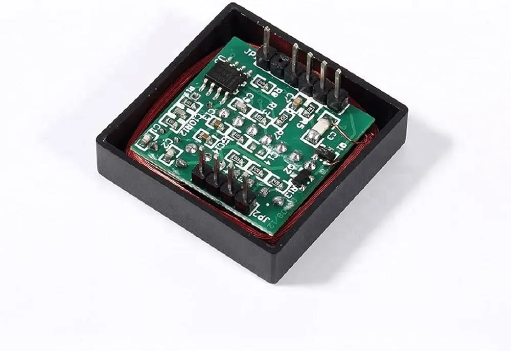
RF PCB refers to printed circuit boards engineered for radio frequency signals, typically in the 2.4 GHz band used by Wi-Fi and Bluetooth in e-readers. These boards require specialized layouts to maintain signal integrity over short distances while minimizing power consumption. In e-readers, poor RF PCB design leads to weak connectivity, increased latency, or excessive battery drain during wireless sessions. Engineers prioritize RF PCB optimization to achieve compliance with performance expectations in consumer electronics. The compact form factor amplifies challenges, as components must coexist with displays and processors without mutual interference. Ultimately, effective RF PCB design extends device usability and reliability in real-world environments.
Core Principles of Antenna Design in RF PCBs
Antenna design forms the cornerstone of RF PCB functionality, converting electrical signals to electromagnetic waves for wireless transmission. In e-readers, planar inverted-F antennas (PIFAs) or meander line antennas suit the slim profile, offering compact footprints with reasonable efficiency. Placement near board edges avoids enclosure shielding, while clearance areas prevent detuning from nearby metal. Substrate thickness and dielectric constant influence radiation patterns, requiring simulation for resonance at target frequencies. Ground plane size acts as a reflector, enhancing gain but demanding careful shaping to suppress surface waves. Adhering to design guidelines ensures antennas meet gain and bandwidth needs without external components.
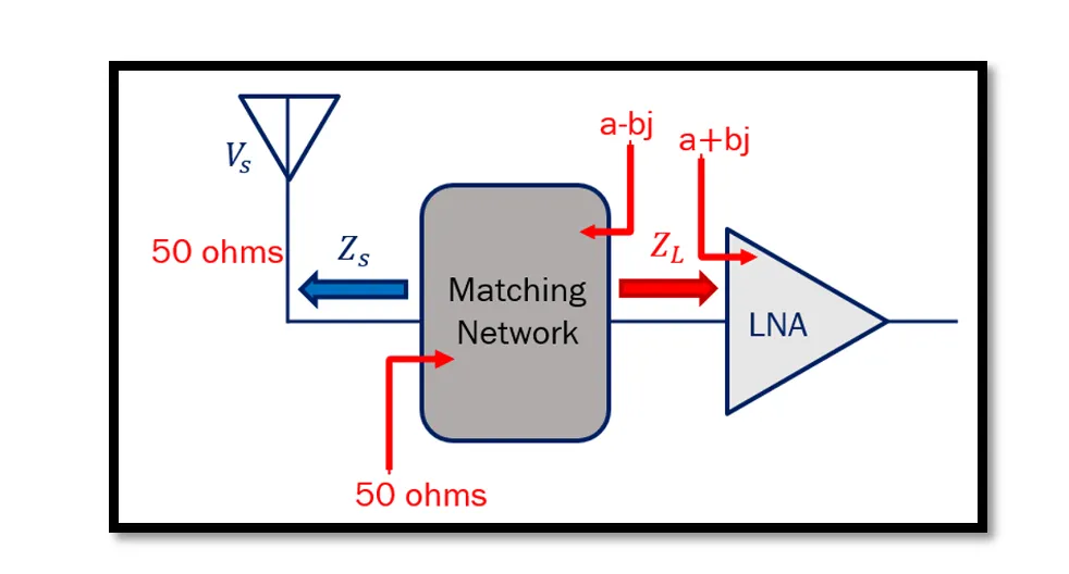
Impedance Matching Techniques for RF PCBs
Impedance matching aligns transmission line characteristics with antenna and component impedances, maximizing power transfer and minimizing reflections. In RF PCBs for e-readers, 50-ohm microstrip traces serve as standard lines, calculated using width, thickness, and dielectric properties. Pi-networks or L-networks with inductors and capacitors provide tunable matching, adjusted via Smith chart analysis for complex conjugates. Via transitions and bends introduce discontinuities, necessitating compensation like mitered corners or stubs. Fabrication tolerances affect matching, so controlled processes maintain line consistency. Proper impedance matching reduces VSWR, preserving signal strength across the wireless chain.
According to IPC-2221 standards, designers must account for these parameters to ensure reliable high-frequency performance.
Signal Amplification Strategies in E-Reader RF PCBs
Signal amplification boosts weak RF signals for transmission or recovers received ones, critical for e-reader range in varied environments. Low-noise amplifiers (LNAs) at the receive path forefront minimize added noise while providing gain. Power amplifiers (PAs) drive antennas, selected for efficiency classes like class-AB to suit battery constraints. Matching networks precede and follow amplifiers to optimize load and source impedances. Thermal management prevents gain compression, using vias for heat dissipation to ground planes. Integration on RF PCBs demands proximity to RF chains, avoiding digital crosstalk.
Noise Reduction Methods for RF PCB Performance
Noise reduction preserves signal-to-noise ratio (SNR) in RF PCBs, where digital switching generates harmonics overlapping wireless bands. Solid ground planes under RF traces shield against coupled noise, with stitching vias forming fences along sensitive paths. Separation zones isolate RF sections from processors and power supplies, routing DC lines orthogonally. Decoupling capacitors near IC pins shunt high-frequency noise to ground. Ferrite beads on supply lines attenuate conducted interference. Multilayer stacks dedicate inner layers to ground, enhancing isolation.
Best Practices for RF PCB Layout in E-Readers
RF PCB layout begins with stackup selection, favoring low-loss dielectrics and consistent thicknesses for controlled impedance. Traces follow curved paths to minimize radiation, with lengths under quarter-wavelength at operating frequencies. Component placement groups RF blocks contiguously, prioritizing signal flow from transceiver to antenna. Power distribution uses wide pours for low inductance, bypassed extensively. DFM considerations include solder mask openings for fine-pitch RF parts and test points for S-parameter verification. Fabrication aligns with IPC-6018 qualification requirements for high-frequency boards.
Troubleshooting Common RF PCB Issues in E-Readers
E-reader RF PCBs often face detuning from enclosure proximity, resolved by modeling interactions early. Excessive insertion loss traces to rough copper or dielectric absorption, addressed via smoother finishes and material specs. Radiation from digital clocks causes spurs, mitigated by spread-spectrum clocks and filtering. Poor battery life signals inefficient amplification, tuned via PA bias optimization. Field failures highlight assembly defects like cold solder joints on RF passives, inspected per IPC-A-600 criteria. Systematic debugging with VNAs and spectrum analyzers pinpoints root causes.
Conclusion
Optimizing RF PCB design for e-readers demands integrated attention to antenna design, impedance matching, signal amplification, and noise reduction. These elements ensure robust wireless connectivity in power-sensitive, compact devices. Engineers applying structured layouts and standards achieve superior performance metrics. Future iterations may leverage advanced materials, but fundamentals remain key. Prioritizing these practices yields reliable, efficient e-readers ready for modern wireless demands.
FAQs
Q1: What role does antenna design play in RF PCB for e-readers?
A1: Antenna design in RF PCB determines radiation efficiency and bandwidth for Wi-Fi and Bluetooth. Compact types like PIFAs fit e-reader constraints, requiring ground clearance and resonance tuning. Proper integration avoids detuning from nearby components. This ensures stable connectivity without external antennas.
Q2: How do you achieve impedance matching in RF PCB layouts?
A2: Impedance matching in RF PCB uses networks like pi or T configurations to conjugate-match 50-ohm lines to antennas. Trace dimensions control characteristic impedance, verified with simulations. Discontinuities from vias demand compensation. This practice minimizes reflections and maximizes power transfer in wireless paths.
Q3: Why is noise reduction critical for e-reader RF PCB performance?
A3: Noise reduction in RF PCB prevents digital interference from degrading SNR in wireless signals. Ground planes and via stitching isolate sections effectively. Decoupling and separation zones suppress coupling. These techniques maintain link margins for reliable e-reader connectivity.
Q4: What are best practices for signal amplification on RF PCBs?
A4: Signal amplification on RF PCBs employs LNAs and PAs with matching networks for gain and efficiency. Placement near RF chains reduces losses, while thermal vias manage heat. Bias optimization suits low-power e-readers. This balances range and battery life effectively.
References
IPC-2221 — Generic Standard on Printed Board Design. IPC, 2012
IPC-2252 — Design Guide for RF/Microwave Circuit Boards. IPC, 2002
IPC-6018D — Qualification and Performance Specification for High Frequency (Microwave) Printed Boards. IPC, 2017


