Why is Signal Integrity Crucial in Audio Amplifier PCBs?
In audio electronics, the quality of sound from an amplifier hinges entirely on signal integrity. This term describes how well an electrical signal maintains its original characteristics as it travels through a circuit. For audio amplifiers, even minor signal degradation can manifest as unwanted noise, distortion, or interference, fundamentally detracting from the listening experience.
Audio signals typically cover the entire range of human hearing, from 20 Hz to 20 kHz. Preserving the integrity of these signals across such a broad spectrum is essential for accurate sound reproduction. Issues like crosstalk, impedance mismatches, and incorrect trace routing are common culprits that introduce undesirable noise or lead to signal loss. By meticulously applying proper PCB design principles, these problems can be significantly mitigated, ensuring the amplifier’s output faithfully matches its input.
What Are the Fundamental Principles for Routing Audio Signals on a PCB?
Effective signal routing on an audio amplifier PCB is akin to designing an optimal path for sound. Just as a smooth road ensures a comfortable journey, well-planned traces guarantee signal purity. Adhering to foundational principles ensures audio signals travel efficiently and without degradation.
Keep Signal Paths Short and Direct
Long signal traces can inadvertently act as antennas, making them susceptible to picking up electromagnetic interference (EMI) from adjacent components or external sources. To counter this, it’s vital to keep audio signal paths as concise and direct as possible. Components critical to the signal path, such as input capacitors and resistors, should be placed in close proximity to the amplifier chip or transistor. This practice effectively shortens trace lengths, reduces impedance, and helps preserve overall signal integrity. For instance, in a preamp stage, positioning input components within half an inch of the amplifier’s input pins can significantly minimize noise pickup.
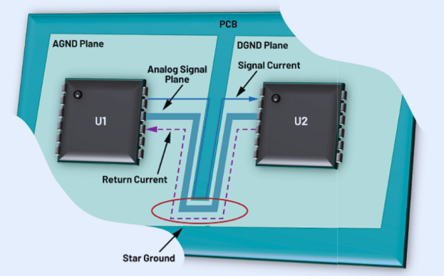
Separate Analog and Digital Sections
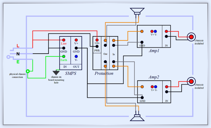
Modern audio amplifiers frequently integrate both analog and digital circuitry, often including microcontrollers for control. Mixing these diverse signal types can lead to crosstalk, where digital switching noise infiltrates and compromises sensitive analog audio signals. To prevent this, it is crucial to physically segregate the analog and digital sections on the PCB. This separation often involves using distinct ground planes for each type of circuit, connecting them at a single, designated point—a method known as "star grounding." This approach effectively isolates digital noise, ensuring the audio signal remains pure. For designs with limited space, a multilayer PCB can be employed, dedicating separate layers specifically for analog and digital signals.
How Does Impedance Matching Impact Audio Amplifier Performance?
Impedance matching is a cornerstone of efficient signal transfer in electronic circuits, particularly critical in audio amplifier PCBs. It ensures that the characteristic impedance of the signal source, the PCB trace, and the load are compatible, thereby facilitating maximum power transfer and minimizing unwanted signal reflections. Without proper impedance matching, an audio system can suffer from signal loss and distortion, issues that become even more pronounced with higher frequency signals.
The Importance of Impedance Alignment
In audio systems, common speaker impedances range from 4 to 8 ohms, yet amplifier outputs and PCB traces may possess different impedance values. A mismatch causes energy to reflect back towards the source, creating standing waves that can audibly distort the audio. This effect is particularly detrimental for frequencies above 10 kHz, where signal integrity is easily compromised by reflections.
Practical Steps for Achieving Impedance Matching
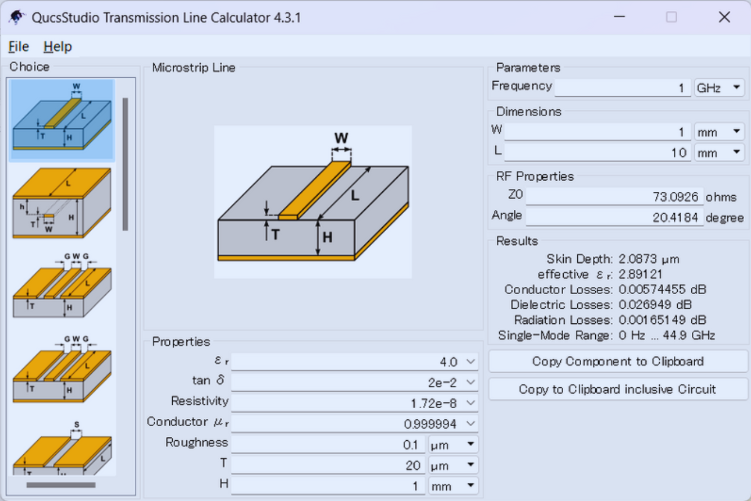
To achieve effective impedance matching, designers must calculate the characteristic impedance of PCB traces and ensure alignment with connected components. For microstrip traces, the characteristic impedance (Z₀) can be calculated using a specific formula: Z₀ = (87 / √(Ɛr + 1.41)) * ln(5.98 * h / (0.8 * w + t)). Here, Ɛr is the dielectric constant of the PCB material (around 4.5 for FR-4), h is the dielectric layer height, w is the trace width, and t is the trace thickness—all typically measured in mils. For audio amplifier PCBs, the goal is often to match trace impedance closely to the load, such as 8 ohms for a speaker. Adjusting trace width and layer spacing during the design phase allows for precise tuning. Many contemporary PCB design software suites offer integrated impedance calculators to simplify this complex process.
How Does Trace Width Affect Signal Integrity and Current Capacity?
Trace width is a dual-function parameter in audio amplifier PCB design, influencing both the current-carrying capability of a conductor and the impedance of the signal path. Selecting the correct trace width is fundamental for upholding signal integrity and preventing localized overheating.
Selecting Appropriate Trace Widths
For the audio signal paths themselves, which typically carry low currents, a trace width between 10 to 20 mils (0.010-0.020 inches) is generally adequate. However, power delivery lines for the amplifier demand significantly wider traces. These larger widths are necessary to handle higher currents without experiencing detrimental voltage drops or excessive heat buildup. Utilizing a trace width calculator, designers can determine the precise dimensions required based on expected current levels and acceptable temperature rise. For example, a 1-amp current on a standard 1 oz copper PCB might necessitate a 50-mil trace to keep its temperature rise below 10°C.
Impact on High-Frequency Audio Signals
When dealing with higher frequency signals, narrower traces can inadvertently increase impedance, which in turn can lead to signal loss. A careful balance must be struck by keeping such traces short and employing the impedance calculation formulas to fine-tune their width. Maintaining consistency in trace width across a signal path is also crucial, as sudden changes in width can cause impedance discontinuities, resulting in signal reflections that degrade audio quality.
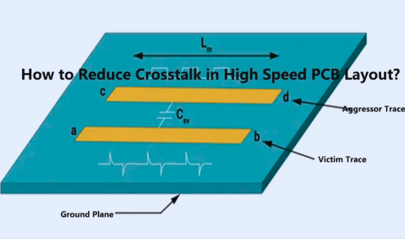
Effective Strategies for Minimizing Crosstalk in Audio PCBs
Crosstalk, the undesired interference between signals on adjacent traces due to electromagnetic coupling, poses a significant threat to audio quality in amplifier PCBs. It can introduce unwanted noise or blend different audio channels, severely degrading the clarity of the output.
Design Techniques to Reduce Crosstalk
Several proven design techniques can effectively minimize crosstalk. One crucial strategy is to increase trace spacing, adhering to the "3W rule," which recommends maintaining a gap of at least three times the trace width between parallel signal traces. For instance, a 10-mil trace should have a 30-mil gap. Another powerful method involves the use of ground planes; placing a solid ground plane beneath signal traces provides an electromagnetic shield, absorbing stray fields and protecting signals from interference. In multi-layer PCB designs where space is at a premium, routing sensitive audio signals on different layers, separated by a dedicated ground plane, can effectively isolate them. Furthermore, avoiding parallel routing where possible, and instead routing traces perpendicularly, significantly reduces the length over which traces can couple. By implementing these strategies, designers can substantially reduce crosstalk, ensuring each audio channel remains distinct and clear.
Suggested Reading: Crafting Clarity: Essential Techniques for Low-Noise Audio Amplifier PCBs
Managing High-Frequency Signals in Audio Amplifier Designs
While the core audio spectrum is relatively low frequency, modern audio amplifier PCBs often incorporate high-frequency elements such as switching power supplies or digital processing units. These high-frequency signals are particularly susceptible to issues like reflection, electromagnetic interference (EMI), and crosstalk, which can severely impact audio fidelity.
Challenges Posed by High Frequencies
At frequencies exceeding 100 kHz, PCB traces begin to behave more like transmission lines. In this regime, even minor impedance mismatches can lead to significant signal reflections. Moreover, the high-frequency noise generated by switching regulators can easily couple into sensitive audio traces, resulting in audible interference.
Best Practices for High-Frequency Routing
To mitigate these challenges, several best practices are essential. Designers should employ controlled impedance traces for high-frequency signals, typically targeting a specific impedance (e.g., 50 ohms) using the previously discussed formulas, to prevent reflections and signal loss. The strategic placement of decoupling capacitors (e.g., 0.1 μF) near the power pins of high-frequency components is crucial for filtering noise and stabilizing voltage. Furthermore, minimizing loop areas by keeping power and ground traces close together reduces EMI radiation. Finally, isolating high-frequency components, such as switching power supplies, by physically separating them from the sensitive audio signal paths, is paramount to prevent unwanted interference. Careful management of these elements ensures that high-frequency operations do not degrade the overall audio performance.
Optimal Grounding Techniques for Noise-Free Audio
Proper grounding is perhaps the most critical aspect of audio amplifier PCB design for achieving noise-free operation. A poorly designed ground system can introduce common issues such as ground loops, which often manifest as a pervasive low-frequency hum in the audio output, significantly detracting from sound quality.
Implementing Star Grounding
To minimize noise, implementing a star grounding scheme is highly recommended. In this approach, all individual ground connections converge at a single, central point. This design prevents return currents from different sections of the circuit from sharing common ground paths, which is a primary cause of induced noise. For example, the grounds from the input stage, the output power stage, and the power supply should all connect to one central point, typically situated near the main power input. This centralized connection acts as a reference point, effectively isolating noise.
Utilizing Ground Planes for Shielding
For multi-layer PCBs, dedicating an entire layer to a solid ground plane offers substantial benefits. This ground plane provides a low-impedance return path for currents and acts as an effective shield, protecting sensitive traces from external and internal noise. It is crucial to ensure this ground plane remains unbroken beneath critical audio signal paths to maximize its shielding effectiveness and maintain a stable reference. The integrity of this plane directly correlates with the suppression of unwanted noise and interference.
Final Considerations for Superior Audio Amplifier PCB Design
Crafting an audio amplifier PCB with exceptional signal integrity demands meticulous attention to detail and unwavering adherence to established best practices. Beyond the core routing techniques, several additional considerations can significantly enhance performance and reliability.
One vital step is to simulate your design using advanced PCB design software. This allows for the early identification of potential issues like crosstalk or impedance mismatches, preventing costly revisions after manufacturing. Once simulations are complete, testing prototypes with actual audio signals is indispensable; this real-world evaluation can uncover subtle noise or distortion that might have been overlooked in simulations. Choosing high-quality PCB materials with consistent dielectric properties is also crucial, as this directly impacts impedance control and overall signal fidelity. Lastly, always ensure that power supply traces are wide and short; this minimizes voltage drops, which could otherwise negatively affect the amplifier's stable operation and performance.
Achieving Pristine Sound Through Strategic PCB Routing
Signal integrity stands as the foundational pillar for any high-performance audio amplifier PCB. By skillfully applying audio amplifier PCB signal routing techniques—including precise impedance matching, appropriate trace width selection, effective crosstalk minimization, and meticulous management of high-frequency signals—designers can create products that deliver truly exceptional sound quality. A well-thought-out layout, robust grounding strategies, and the careful separation of various signal types are the most potent tools available to eliminate unwanted noise and distortion.
Regardless of whether the project involves a straightforward stereo amplifier or an intricate multi-channel audio system, these principles will serve as an invaluable guide towards successful design outcomes. Implement these strategic routing techniques in your forthcoming projects, and personally experience the transformative impact of achieving crystal-clear sound.