What is ECU PCB Layer Stackup Design?
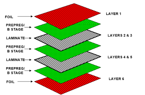
ECU PCB layer stackup design refers to the precise configuration of conductive copper layers interspersed with insulating dielectric materials within a printed circuit board specifically engineered for automotive Electronic Control Units. These ECUs are the brains behind critical vehicle operations, overseeing functions such as engine management, braking systems, advanced driver-assistance systems (ADAS), and infotainment. The stackup fundamentally dictates the number of layers in the PCB, the designated role of each layer (e.g., carrying signals, distributing power, or providing a ground reference), and their physical separation to prevent electromagnetic interference (EMI) and ensure optimal electrical performance.
A typical ECU PCB often incorporates 4, 6, or 8 layers, with the choice depending directly on the system's complexity and component density. For instance, a 4-layer stackup might feature outer signal layers and internal power and ground planes, effectively shielding signals from EMI. The overarching objective of a meticulously designed stackup is to enhance signal integrity, efficiently manage power distribution, and consistently meet the stringent reliability standards demanded by automotive environments. These environments typically involve operating temperatures ranging from -40°C to 125°C and constant exposure to vibrations, making robust design paramount.
Why Layer Stackup is Critical for ECU Performance
The layer stackup serves as the foundational architecture of any ECU PCB. A poorly conceived stackup can lead to a cascade of detrimental effects, including unacceptable levels of signal crosstalk, significant power supply noise, and even outright system failure—all of which are intolerable in automotive applications where operational safety and reliability are non-negotiable.
Ensuring Signal Integrity
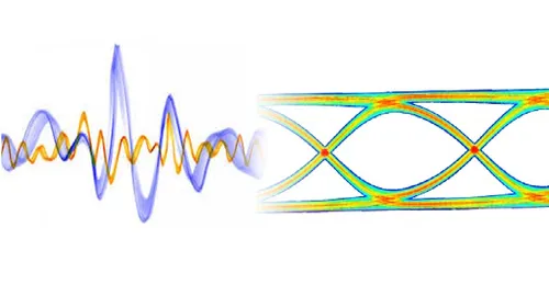
High-speed signals prevalent in ECUs, such as those used for CAN bus communication (which can reach 1 Mbps for CAN 2.0 and up to 5 Mbps for CAN FD), necessitate meticulously controlled impedance to prevent signal distortion and maintain data fidelity. A properly engineered stackup ensures that signal traces are consistently routed adjacent to solid ground planes. This proximity is critical for maintaining consistent impedance values, often targeting 50 ohms for single-ended traces and 90 ohms for differential pairs, thereby minimizing signal reflections and degradation.
Suggested Reading: Understanding Signal Integrity Issues in High-Speed ECU PCBs
Optimizing Power Integrity
ECUs frequently manage multiple voltage levels concurrently (e.g., 3.3V for microcontrollers and 12V for various actuators). The incorporation of dedicated power planes within the stackup is crucial for minimizing voltage drops and suppressing noise, which collectively ensures a stable and reliable power supply across the board.
Suggested Reading: Implementing Power Integrity Analysis for Efficient ECU PCB Design
Mitigating Electromagnetic Interference (EMI)
Automotive environments are inherently noisy, characterized by significant EMI generated by electric motors, various switches, and other electronic systems. A well-designed stackup, featuring continuous ground planes strategically positioned adjacent to signal layers, is essential for minimizing EMI. These ground planes provide low-impedance return paths for high-frequency currents and effectively shield sensitive signals from external electromagnetic disturbances.
Enhancing Thermal Management
ECUs, particularly in high-power applications such as electric vehicle control units, generate a considerable amount of heat. Stackups designed with thicker copper layers (e.g., 2 oz copper instead of the standard 1 oz) or incorporating dedicated thermal vias can significantly improve heat dissipation capabilities, thereby preventing localized overheating and ensuring long-term operational stability.
Key Considerations in ECU PCB Layer Stackup Design
Designing an effective layer stackup for an ECU PCB requires a delicate balance of multiple interdependent factors to meet the rigorous performance and reliability objectives demanded by automotive applications.
Determining the Optimal Number of Layers
The number of layers required for an ECU PCB is primarily driven by the complexity of the electronic circuit and the density of components. A simpler ECU, perhaps for controlling basic functions like power windows, might effectively use a 4-layer board. In contrast, a sophisticated engine management system or an ADAS controller could necessitate 8 or more layers to accommodate its complexity.
● 4-Layer Stackup: Commonly employed for less complex ECUs. A typical configuration positions signal layers on the top and bottom, with dedicated internal power and ground planes sandwiched in between. This arrangement provides fundamental shielding for the external signal traces.
● 6-Layer Stackup: Suitable for mid-range ECUs that have a moderate density of signals. A common and effective configuration is Signal-Ground-Signal-Power-Ground-Signal. This offers superior EMI shielding and enhanced control over signal impedance compared to a 4-layer design.
● 8+ Layer Stackup: Reserved for advanced ECUs handling high-speed signals and managing multiple distinct power domains. These more complex stackups allow for the dedicated routing of different signal types (e.g., separating analog sensor signals from high-speed digital communication lines) and the inclusion of additional ground planes for superior noise isolation.
Strategic Layer Arrangement for Signal and Power Integrity
The precise arrangement of layers is fundamental to achieving robust signal and power integrity, which are non-negotiable for reliable ECU operation.
● Adjacent Ground Planes: It is best practice to place continuous ground planes directly adjacent to signal layers. This configuration provides an ideal low-impedance return path for high-speed signals, which is critical for minimizing signal reflections and reducing crosstalk between traces.
● Power Plane Placement: Position power planes in close proximity to ground planes. This creates a low-inductance path that is essential for the effective functioning of decoupling capacitors, thereby significantly minimizing power supply noise and voltage ripple.
● Signal Layer Separation: Route high-speed or sensitive signals on outer layers or ensure they are well-separated from noisy power distribution lines to prevent inductive or capacitive interference. For example, maintaining distinct layers for analog sensor signals versus digital communication lines is often recommended.
For a 6-layer board, an optimized stackup for signal and power integrity might be structured as: Top Signal, Ground, Inner Signal 1, Power, Ground, Bottom Signal. This design ensures that every signal layer benefits from an immediate adjacent reference plane, which is crucial for achieving controlled impedance.
Achieving Automotive PCB Impedance Control
Impedance control is a cornerstone of high-speed ECU design. Any mismatch in impedance can cause detrimental signal reflections, leading to data errors in critical systems like ABS, engine control, or steer-by-wire. To achieve precise and consistent impedance (e.g., 50 ohms for single-ended traces or 90 ohms for differential pairs), consider these factors:
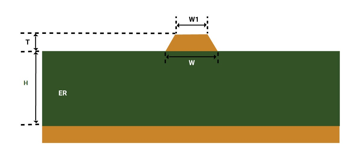
● Trace Width and Spacing: Utilize specialized PCB design software to accurately calculate trace dimensions (width and spacing) based on the dielectric constant of the chosen material and the thickness of the dielectric layers. For example, on a 1.6mm thick FR-4 board (with a dielectric constant of approximately 4.4), a 50-ohm trace on the top layer with an immediate ground plane beneath it might require a width around 0.3mm.
● Dielectric Thickness: Thinner dielectric layers positioned between signal traces and their reference planes generally result in tighter impedance control. However, this often correlates with increased manufacturing costs due to the higher precision required.
● Continuous Reference Planes: It is imperative that high-speed signal traces are routed over continuous and uninterrupted ground or power planes. Avoid routing such traces over split planes, as discontinuities in the return path can create impedance mismatches and degrade signal quality.
Impedance control is especially vital for modern automotive communication protocols like CAN FD or Automotive Ethernet, where data rates can easily exceed 5 Mbps. Even a minor impedance mismatch, as small as 10%, can noticeably degrade signal quality, potentially leading to critical communication failures.
Material Selection for ECU Applications
The selection of PCB materials for ECUs is paramount due to the exceptionally harsh operating conditions encountered in automotive environments. The chosen substrate and copper thickness must be capable of enduring extreme temperature fluctuations, high humidity levels, and constant mechanical stress and vibration.
● FR-4 Variations: Standard FR-4 is a common, cost-effective material for many ECU PCBs due to its generally good electrical properties. However, for applications exposed to higher temperatures (above 105°C), high-Tg (glass transition temperature) FR-4, with a Tg of 170°C or higher, is frequently the preferred choice, offering enhanced thermal stability.
● Polyimide: This material is often specified for high-reliability ECUs that require exceptional thermal stability (capable of withstanding up to 260°C) and inherent flexibility. While offering superior performance, polyimide-based PCBs are typically more expensive than FR-4 alternatives.
● Copper Thickness: Automotive HDI PCBs frequently utilize thicker copper layers, such as 1 oz (35 µm) or 2 oz (70 µm), rather than thinner options. This increased copper weight provides improved current-carrying capacity, crucial for power-heavy ECUs, and significantly enhances heat dissipation capabilities.
● Thermal Conductivity: For high-current applications within ECUs, particularly those generating substantial heat, materials with higher thermal conductivity are beneficial. In some extreme power ECU designs, metal-core PCBs may be employed to maximize heat management.
Selecting the correct materials ensures that the PCB can reliably perform within the demanding automotive environment while consistently maintaining its specified electrical characteristics. For example, an ECU designed for an electric vehicle's battery management system would likely require a high-Tg material to cope with elevated temperatures in proximity to the battery pack.
Best Practices for Robust Automotive PCB Stackup Design
To ensure optimal performance and reliability in ECU PCBs, adhere to these best practices throughout the design and manufacturing phases:
● Thorough Pre-Manufacturing Simulation: Before committing to physical manufacturing, utilize advanced simulation tools to accurately model and analyze the signal integrity, power distribution networks, and thermal behavior of your proposed stackup. This proactive approach helps identify and rectify potential issues, such as impedance mismatches or localized hot spots, during the design phase rather than in costly prototyping or production.
● Minimize Layer Transitions for High-Speed Signals: Whenever feasible, route high-speed signals entirely on a single PCB layer. This minimizes the necessity for vias, which inherently introduce additional inductance and capacitance into the signal path, thereby degrading signal quality and complicating impedance control.
● Implement Symmetrical Stackups: Design the PCB layer stackup to be symmetrical around its central axis. This means ensuring that dielectric thicknesses and copper weights are balanced on either side. Symmetrical stackups are crucial for preventing undesirable warpage during the high-temperature manufacturing processes and maintaining board flatness under thermal stress during operation.
● Early Collaboration with Fabricators: Establish close collaboration with your chosen large PCB manufacturer early in the design cycle. Discuss your stackup design in detail, including specifications for dielectric materials, layer thicknesses, and copper weights. This partnership ensures that the design is not only manufacturable but also cost-effective and aligns with the fabricator's capabilities and processes.
● Adherence to Industry Standards: Rigorously follow relevant automotive industry standards. This includes functional safety standards like ISO 26262 and PCB qualification standards such as IPC-6012. Adherence to these standards is critical for ensuring the overall reliability, safety, and regulatory compliance of your ECU designs.
Challenges in ECU PCB Layer Stackup Design
Designing an effective layer stackup for automotive ECUs is a complex undertaking, often involving challenging trade-offs between performance, cost, and manufacturability. Engineers frequently encounter several common hurdles:
● Severe Space Constraints: Modern vehicle architectures demand increasingly compact electronic modules. This forces designers to create high-density stackups, often incorporating thinner dielectric layers, which in turn can significantly increase manufacturing complexity and cost.
● Demanding High-Speed Requirements: As automotive systems increasingly adopt faster and more complex communication protocols (e.g., Automotive Ethernet operating at 100 Mbps or even higher), maintaining pristine signal integrity becomes an exponentially more challenging task, requiring exceptionally precise impedance control and advanced routing techniques.
● Intense Cost Pressures: The automotive industry is highly competitive, characterized by constant pressure to achieve high reliability while maintaining low unit costs. This economic reality often imposes strict limitations on material choices and the maximum number of layers that can be incorporated into an ECU PCB design.
● Extreme Environmental Stress: ECUs are expected to perform flawlessly and reliably under a broad spectrum of severe environmental conditions, including wide temperature swings, high humidity, continuous vibration, and potential exposure to various chemicals. These demands push the boundaries of standard PCB materials and conventional stackup designs, requiring innovative solutions.
Overcoming these multifaceted challenges necessitates meticulous planning, the strategic deployment of advanced PCB design and simulation tools, and robust collaboration with experienced PCB fabricators who possess a deep understanding of specific automotive requirements and manufacturing constraints.
Conclusion: Building Reliable ECU PCBs with Optimal Stackup Design
A meticulously designed layer stackup forms the bedrock of high-performance ECU PCBs, which are critical components in modern automotive applications. By strategically selecting the appropriate number of layers, optimizing their arrangement, implementing precise automotive PCB impedance control, and making informed material selections, engineers can effectively ensure robust signal and power integrity. This comprehensive approach enables the successful fulfillment of the stringent and rigorous demands characteristic of the automotive operating environment. Whether you are developing a straightforward 4-layer board for a basic control unit or an advanced 8-layer design for a state-of-the-art autonomous driving system, the fundamental principles of ECU PCB layer stackup design remain constant: an unwavering prioritization of performance, reliability, and manufacturability.
Here at AIVON, we are deeply committed to providing comprehensive support for your automotive PCB projects through high-quality manufacturing services and expert technical guidance. From the initial stages of stackup design conception to the final production run, our dedicated team is prepared to assist you in achieving optimal ECU performance. Embark on your next project with absolute confidence, secure in the knowledge that every layer of your PCB is meticulously engineered for unparalleled success and enduring reliability.