Introduction
Avionics systems operate in environments where signal integrity directly impacts flight safety and mission success. Printed circuit boards (PCBs) in these systems handle high-speed digital signals, analog interfaces, and RF communications under extreme conditions like vibration, temperature fluctuations, and electromagnetic interference. Poor avionics PCB signal integrity can lead to data errors, timing violations, or complete system failures. Engineers must prioritize layout strategies that maintain signal quality from source to receiver. This article explores key challenges and proven optimization techniques for avionics PCB layouts. By focusing on controlled impedance, crosstalk mitigation, reflection control, and robust grounding, designers can ensure reliable performance.
Why Signal Integrity Matters in Avionics PCBs
Signal integrity refers to the preservation of electrical signal quality throughout its propagation across the PCB. In avionics, where systems process radar data, flight controls, and sensor fusion at gigabit speeds, any degradation compromises real-time decision-making. Unlike consumer electronics, avionics PCBs demand Class 3 quality levels per IPC standards to withstand lifecycle stresses. Factors like trace impedance mismatches or noise coupling amplify risks in compact, multilayer boards. Engineers targeting avionics PCB signal integrity must integrate these considerations early in the design phase. Ultimately, optimized layouts reduce bit error rates and enhance overall system reliability.
Avionics environments exacerbate signal integrity issues due to power supply noise from switched-mode converters and EMI from nearby antennas. High layer counts in modern boards increase coupling risks between signal planes. Compliance with IPC-2221 guidelines for conductor spacing and routing helps mitigate these from the outset. Without proactive measures, signals distort, leading to eye diagram closure and protocol timeouts. Procurement teams specify these traits to align manufacturing with design intent.
Key Technical Principles of Avionics PCB Signal Integrity
Signal propagation on PCBs behaves as transmission lines when rise times approach or exceed trace delay times. Characteristic impedance, determined by trace geometry, dielectric constant, and layer spacing, governs wave behavior. Mismatches cause reflections that superimpose on the original signal, distorting edges and introducing jitter. Crosstalk arises from capacitive and inductive coupling between adjacent traces, injecting noise into victim lines. In avionics PCB signal integrity, these effects compound at frequencies above 500 MHz. Understanding these principles enables precise layout control.
Dielectric materials with low loss tangents minimize attenuation, while uniform thickness ensures consistent impedance. Trace width and spacing trade off against routing density, requiring stackup optimization. Ground return paths influence loop inductance, affecting both emissions and susceptibility. Reflections partially return based on the reflection coefficient, calculated as (Z_load - Z0)/(Z_load + Z0). Engineers simulate these interactions to predict behavior before fabrication.
Achieving Controlled Impedance in Avionics PCBs
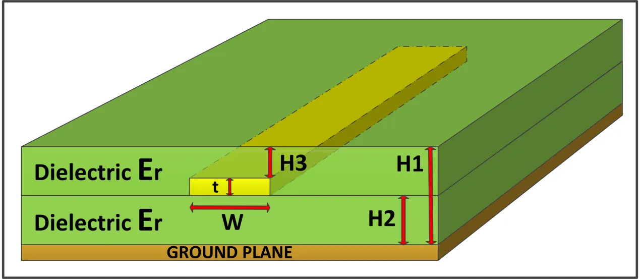
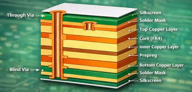
Controlled impedance avionics PCBs maintain trace characteristic impedance within tight tolerances, typically ±10% or better for high-speed nets. Stackup design starts with selecting core and prepreg thicknesses to position signal layers symmetrically around ground planes. Microstrip traces on outer layers offer easier access but higher radiation; striplines embedded between planes provide better shielding. Width calculators based on IPC-2141 principles guide initial dimensions, accounting for copper weight and etch factors. Fabrication tolerances demand verification coupons on panels. This approach ensures signals launch cleanly without initial reflections.
Layer pairing, such as signal-ground-signal, confines fields and stabilizes impedance. Asymmetric stacks introduce skew between layers, complicating length matching. Engineers iterate stackups using field solvers to hit targets like 50 ohms single-ended or 100 ohms differential. Plating buildup in vias alters local impedance, necessitating back-drilling or blind vias. For avionics, polyimide or high-Tg FR-4 laminates support controlled impedance under thermal cycling.
Crosstalk Reduction Techniques in Avionics PCBs
Crosstalk reduction in avionics PCBs relies on minimizing mutual capacitance and inductance between aggressor and victim traces. Increase edge-to-edge spacing to at least 3-5 times the trace width for critical nets, reducing near-end and far-end coupling. Orthogonal routing on adjacent layers aligns electric fields perpendicularly, slashing inductive crosstalk. Guard traces tied to ground absorb noise, though they consume real estate. Differential pairs benefit from tight coupling within the pair and wide separation from others. These strategies preserve signal margins in dense layouts.
Routing high-speed signals away from clocks and power planes further isolates them. Stitching vias along trace edges connect ground planes, providing low-impedance return paths. Length staggering prevents simultaneous switching that amplifies coupling. Simulations quantify peak noise voltage, guiding spacing rules. In practice, these yield over 20 dB isolation without heroic measures.
Minimizing Signal Reflections in Avionics PCBs
Signal reflection in avionics PCBs stems from impedance discontinuities at vias, bends, connectors, and terminations. Maintain uniform trace width through transitions, using teardrops at pads to smooth fields. Via optimization includes larger antipads and stub removal via back-drilling for frequencies above 1 GHz. Length-matched routing equalizes delays in buses, preventing skew-induced reflections. Series or parallel termination matches source or load impedance, absorbing energy. Source termination suits point-to-point links common in avionics.
Corner radii of at least 3:1 aspect ratio on bends preserve impedance. Connector pin assignments group pairs with adjacent grounds. Pre-emphasis drivers compensate for losses, but layout primacy avoids reliance. IPC-6012 qualification verifies these post-fabrication through electrical testing. Coordinated efforts yield clean TDR responses.
Grounding Techniques for Avionics PCBs
Grounding techniques for avionics PCBs form the backbone of signal integrity by providing stable reference planes and return currents. Full copper pours on inner layers act as ground planes, minimizing loop areas for differential-mode currents. Stitch vias every lambda/20 along edges and splits to equalize potentials. Split planes for analog and digital domains prevent noise bridging, connected at single points near power entry. Via fences around sensitive areas shield fields. These create low-inductance paths essential for GHz signals.
Power-ground plane capacitance decouples supplies inherently. Flood fills on signal layers tie to ground where feasible. Bond wires or chassis connections handle structural integrity grounds. Avoid routing splits under traces to prevent impedance jumps. Robust grounding slashes EMI susceptibility in avionics bays.
Best Practices for Integrated Layout Optimization
Integrate these elements through iterative design: start with stackup, route critical nets first, then fill. Symmetry in layer usage balances warpage and CTE mismatches. Thermal vias under power devices aid heat spreading without integrity hits. DFM checks flag narrow spaces or unconnected pours. Post-layout extraction feeds SI simulations for validation. Documentation specifies impedance targets and test points.
Multiboard systems require connector SI analysis. Hybrid materials blend high-speed and rigid sections seamlessly. Qualification per IPC standards confirms production capability.
Conclusion
Optimizing PCB layout for avionics systems demands a holistic grasp of signal integrity principles. Controlled impedance avionics PCBs, coupled with crosstalk reduction in avionics PCB designs, reflection control, and solid grounding techniques for avionics PCBs, deliver mission-critical performance. Engineers applying these structured approaches minimize risks in high-stakes environments. Proactive simulation and standards adherence accelerate reliable deployments. Future trends like higher data rates will intensify these needs, rewarding early mastery.
FAQs
Q1: What factors most impact avionics PCB signal integrity?
A1: Avionics PCB signal integrity hinges on impedance control, crosstalk from adjacent traces, reflections at discontinuities, and ground return quality. Harsh vibration and EMI amplify these, demanding Class 3 IPC-compliant layouts. Stackup symmetry and spacing rules counter dielectric variations. Simulations predict eye heights, guiding refinements for gigabit links.
Q2: How do you implement controlled impedance avionics PCB?
A2: Controlled impedance avionics PCB starts with stackup definition using field solvers for trace widths matching 50/100 ohms. Select low-Dk prepregs and verify with TDR coupons. Symmetric layering around grounds stabilizes values. Fabrication tolerances under ±10% suit high-speed needs. IPC-2141 aids calculations for consistent performance.
Q3: What are effective crosstalk reduction in avionics PCB methods?
A3: Crosstalk reduction in avionics PCB employs wider spacings, orthogonal routing, and guard traces to ground. Stitch planes with vias for tight coupling to returns. Avoid parallel runs over 1 cm. Differential routing enhances immunity. These yield low noise injection in dense signal environments.
Q4: Why are grounding techniques for avionics PCB critical?
A4: Grounding techniques for avionics PCB provide low-impedance returns, reducing inductive noise and EMI. Solid planes and stitching equalize potentials across layers. Splits isolate domains without current loops. This preserves signal margins under power switching. IPC-2221 spacing rules integrate grounding seamlessly.
References
IPC-2221 — Generic Standard on Printed Board Design. IPC
IPC-6012 — Qualification and Performance Specification for Rigid Printed Boards. IPC
IPC-2141 — Design Guide for High-Speed Controlled Impedance. IPC


