Introduction
Avionics systems in aircraft and spacecraft operate under extreme conditions, including high altitudes, rapid temperature fluctuations, and intense vibrations. These environments generate significant heat from power electronics, processors, and RF components mounted on printed circuit boards. Effective thermal management for avionics PCBs is essential to prevent overheating, which can lead to performance degradation, component failure, or system downtime. Thermal vias and heat sinks emerge as critical solutions for heat dissipation in avionics PCBs, enabling reliable operation over extended missions. By channeling heat away from hotspots and increasing surface area for cooling, these techniques ensure compliance with high-reliability requirements. This article explores avionics PCB thermal vias, avionics PCB heat sink design, and integrated strategies for optimal cooling.
Understanding Thermal Vias in Avionics PCBs
Thermal vias are plated through-holes specifically engineered to transfer heat vertically through the PCB stackup, rather than just providing electrical connectivity. In avionics applications, where power densities can exceed standard consumer electronics, these vias connect heat-generating components on the surface to internal copper planes or the opposite side of the board. Arrays of thermal vias, often called via farms, surround hotspots like power ICs or amplifiers to distribute heat evenly and reduce thermal resistance. Without proper avionics PCB thermal vias, localized temperatures rise rapidly, accelerating material degradation and solder joint fatigue. Engineers must consider via diameter, plating thickness, and spacing to balance thermal conductivity with manufacturing feasibility. Adhering to IPC-2221 guidelines ensures these vias enhance reliability without compromising signal integrity.
The mechanism relies on copper's high thermal conductivity, allowing heat to conduct from the component pad through the via barrel to lower layers. Filled thermal vias, where epoxy or conductive paste occupies the core, further improve performance by minimizing air gaps that impede heat flow. In avionics PCB thermal vias design, placement under the thermal pad of surface-mount devices maximizes efficiency. Simulations during the design phase reveal potential bottlenecks, such as via-to-via spacing that could cause solder wicking during assembly. Proper tenting of soldermask over vias prevents solder intrusion while maintaining thermal paths. These practices form the foundation of robust thermal management for avionics PCBs.
The Role of Heat Sinks in Avionics PCB Design
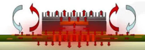
Heat sinks are passive cooling devices attached to PCBs or components to dissipate heat via convection and radiation, expanding the effective surface area for thermal exchange. In avionics PCB heat sink design, extruded aluminum or copper finned structures predominate due to their lightweight properties and corrosion resistance in humid or salty atmospheres. Board-level heat sinks cover large copper pours connected by thermal vias, while component-specific sinks clip directly onto transistors or regulators. The choice depends on available airflow, enclosure constraints, and weight budgets critical in aerospace. Interface materials, such as thermal pads or greases, bridge gaps between the heat source and sink, reducing contact resistance. Effective avionics PCB heat sink design integrates seamlessly with the PCB layout to avoid airflow blockages.
Pin-fin or straight-fin geometries optimize performance based on orientation and boundary conditions, with avionics favoring low-profile designs for compact enclosures. Mechanical attachment methods, including epoxy bonding or spring clips, must withstand vibration without loosening. In thermal management for avionics PCBs, heat sinks complement vias by handling bulk dissipation after initial spreading. Oversized sinks increase capacitance but add mass, requiring trade-offs during system-level thermal analysis. Compliance with IPC-6012 performance specifications verifies that assemblies endure thermal cycling without delamination. These elements ensure heat dissipation in avionics PCBs meets mission-critical demands.
Technical Principles of Heat Transfer in Avionics PCBs
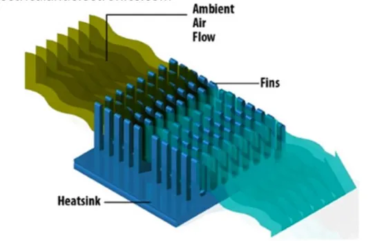
Heat dissipation in avionics PCBs follows conduction, convection, and radiation principles, with conduction dominating through-board paths. Fourier's law governs conduction, where heat flux is proportional to the temperature gradient and material conductivity; copper planes and thermal vias exploit this for rapid lateral and vertical spreading. Junction-to-ambient thermal resistance, theta JA, quantifies overall performance, lowered by parallel thermal paths from vias and sinks. In avionics, low-pressure environments at altitude reduce convection effectiveness, emphasizing radiation and conduction. Multilayer stackups with dedicated power planes act as heat spreaders, fed by avionics PCB thermal vias arrays. Radiation becomes significant for hot surfaces above 100 degrees Celsius, enhanced by emissive coatings on heat sinks.
Convection relies on airflow over finned surfaces, with forced air in some avionics bays boosting Nusselt numbers for better coefficients. Boundary layer thickness influences efficiency, minimized by optimized fin spacing. Radiation follows Stefan-Boltzmann law, proportional to T^4 differences, making black anodized sinks preferable. Integrating these in cooling techniques for avionics PCBs requires finite element analysis to predict hotspots. IPC-2152 provides frameworks for estimating trace heating, extended to via thermal modeling. Understanding these principles guides precise avionics PCB heat sink design.
Best Practices for Integrating Thermal Vias and Heat Sinks
Start with component placement to group heat sources over internal planes connected by thermal vias, promoting even dissipation before heat sink attachment. Use 4 to 9 mil vias in arrays of 10-20 under pads, spaced at 0.5-1 mm to avoid stress concentrations during reflow. Tent unused vias and fill critical ones to prevent voids, enhancing mechanical robustness in vibration-prone avionics. For avionics PCB heat sink design, align fins parallel to expected airflow and ensure at least 10% oversurface coverage for mounting. Thermal interface materials with 1-5 W/mK conductivity minimize gaps, applied uniformly to avoid pump-out under thermal cycling.
Layer stackup optimization dedicates inner layers to ground or power for isothermal spreading, stitched by vias every 5-10 mm. Simulate transient loads to validate steady-state designs, adjusting via counts iteratively. In thermal management for avionics PCBs, hybrid approaches combine embedded coins or heat pipes with external sinks for ultra-high power. Verify via reliability through cross-sectioning per IPC standards, checking plating integrity. Avoid thermal reliefs on vias connected to sinks, as they restrict flow. These practices yield cooling techniques for avionics PCBs that balance performance, manufacturability, and reliability.
Challenges in Avionics PCB Thermal Management and Troubleshooting
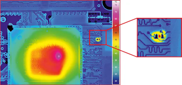
Avionics PCBs encounter challenges like CTE mismatch between components and boards, exacerbated by heat sinks adding mechanical stress. Vibration induces fretting at interfaces, addressed by compliant pads and locking fasteners. High-altitude rarefied air diminishes convection, shifting reliance to conduction via thermal vias. Troubleshooting starts with infrared thermography to map hotspots, followed by via array augmentation. Delamination risks from moisture demand bake-out before assembly, per JEDEC guidelines. Overly dense via farms can wick solder, starving joints; mitigate with staggered patterns.
Altitude derating factors adjust sink sizing, as natural convection drops 50% above 10 km. Electromagnetic interference from power planes requires shielding alongside thermal paths. Case studies show via tenting failures leading to contamination; inspect with automated optical systems. Integrate strain gauges during qualification to correlate thermal loads with reliability. Addressing these ensures sustained heat dissipation in avionics PCBs.
Conclusion
Thermal vias and heat sinks form the backbone of thermal management for avionics PCBs, channeling and radiating heat to maintain operational integrity. Strategic avionics PCB thermal vias arrays spread localized loads, while thoughtfully designed heat sinks handle ambient dissipation. Integrating these with stackup planning and simulations yields resilient designs compliant with industry benchmarks. Engineers benefit from logical application of conduction principles and best practices to overcome avionics rigors. Prioritizing these cooling techniques for avionics PCBs safeguards mission success, extending component lifespans in demanding skies.
FAQs
Q1: What are the primary benefits of using avionics PCB thermal vias in high-power designs?
A1: Avionics PCB thermal vias provide low-resistance paths for vertical heat conduction, reducing junction temperatures by linking surface components to internal planes. They prevent hotspots that degrade solder joints and materials under thermal cycling. Arrays enhance spreading, complementing heat sinks for overall thermal management for avionics PCBs. Proper sizing per design standards ensures reliability without electrical interference. (62 words)
Q2: How does avionics PCB heat sink design impact system reliability?
A2: Avionics PCB heat sink design optimizes surface area for convection and radiation, critical in low-airflow enclosures. Finned structures with thermal interfaces lower theta JA, sustaining performance during peaks. Vibration-resistant mounting prevents detachment, aligning with high-reliability classes. Integration with vias maximizes heat dissipation in avionics PCBs, minimizing failure risks from overtemperature. (58 words)
Q3: What cooling techniques for avionics PCBs combine thermal vias and heat sinks effectively?
A3: Cooling techniques for avionics PCBs pair via farms under hotspots with board-mounted heat sinks for bulk removal. Dedicated planes distribute heat laterally before sink attachment. Simulations validate airflow over fins, avoiding shadows. This hybrid approach excels in compact, high-density layouts, ensuring even temperatures per IPC guidelines. (52 words)
Q4: Why is thermal management critical for heat dissipation in avionics PCBs?
A4: Heat dissipation in avionics PCBs averts failures from thermal runaway, preserving signal integrity and longevity. Extreme environments amplify risks, demanding passive solutions like vias and sinks. Proactive design per standards like IPC-2221 meets qualification thresholds. Reliable thermal paths support continuous operation in flight-critical systems. (48 words)
References
IPC-2221B — Generic Standard on Printed Board Design. IPC, 2012
IPC-6012E — Qualification and Performance Specification for Rigid Printed Boards. IPC, 2017
IPC-2152B — Standard for Determining Current Carrying Capacity in Printed Board Design. IPC, 2023
JEDEC J-STD-020E — Moisture/Reflow Sensitivity Classification of Nonhermetic Surface Mount Devices. JEDEC, 2014


