Introduction
Electromagnetic interference (EMI) poses significant challenges in modern electronic manufacturing, where dense circuitry and high-speed signals amplify susceptibility to noise. As devices operate in increasingly congested frequency spectra, effective shielding becomes essential to maintain signal integrity and ensure compliance with regulatory limits. However, traditional shielding approaches often drive up costs through expensive metal enclosures or specialized components, straining budgets in high-volume production. Engineers must navigate this tension by identifying cost-effective EMI shielding strategies that deliver adequate performance without compromising reliability. This article explores affordable PCB shielding methods and low-cost shielding components tailored for practical implementation. By prioritizing design optimization and economical materials, manufacturers can achieve budget-friendly RF shielding solutions while upholding quality standards.
The push for economical electronic manufacturing underscores the need for shielding that scales with production volumes. High costs from over-engineered shields can erode profit margins, particularly in consumer electronics and automotive applications. Yet, under-shielding risks product failures, rework, and certification delays. Balancing these factors requires a deep understanding of shielding physics and manufacturing constraints. Forward-thinking approaches integrate shielding at the PCB level, minimizing add-on expenses. This enables electric engineers to deliver robust designs that meet performance targets affordably.
Understanding EMI Shielding and Its Critical Role
EMI shielding involves materials or structures that attenuate electromagnetic fields to protect sensitive circuits from external noise or prevent internal emissions from radiating outward. In PCB contexts, it counters conducted and radiated interference across radio frequency (RF) ranges, from kilohertz to gigahertz. Without proper shielding, crosstalk between traces, power supply noise, and external sources like wireless signals degrade performance, leading to data errors or system instability. For electric engineers, mastering shielding principles ensures designs pass electromagnetic compatibility (EMC) tests while controlling costs.
The relevance intensifies in compact assemblies where proximity exacerbates coupling. High-speed digital interfaces, such as those in 5G modules or IoT devices, demand precise attenuation to isolate analog and digital sections. Cost-effective EMI shielding not only mitigates these risks but also supports miniaturization trends. Neglecting it invites field failures, recalls, and liability issues. Thus, integrating affordable PCB shielding methods early in the design cycle yields long-term savings through reduced iterations and faster time-to-market.
Regulatory pressures further amplify its importance. Compliance with emission limits requires verifiable shielding effectiveness, often measured in decibels (dB). Budget-friendly RF shielding solutions allow teams to meet these without premium materials. Engineers benefit from strategies that leverage standard PCB processes, avoiding custom fabrications.
Core Technical Principles of EMI Shielding
Shielding effectiveness (SE) quantifies attenuation via three mechanisms: reflection, absorption, and multiple reflections. Reflection occurs when incident waves bounce off conductive surfaces, dominant at low frequencies where skin depth exceeds material thickness. Absorption dissipates energy as heat within the shield, more effective at higher frequencies due to shallower skin depths. Multiple reflections enhance overall SE in thicker or multilayer shields, though they complicate thin-film applications.
Material selection hinges on conductivity, permeability, and thickness. Copper offers excellent reflection due to high conductivity, while ferrites excel in absorption for magnetic fields. For cost-sensitive designs, aluminum provides a viable alternative with lower density and material expense, though it demands thicker gauges for equivalent performance. Engineers calculate SE using SE = 20 log (Z0 / (2 Zs)) for reflection, where Z0 is free-space impedance and Zs is surface impedance, guiding trade-offs.
Frequency dependence shapes strategy. Low-frequency magnetic fields penetrate conductors easily, necessitating high-permeability mu-metal, but these prove costly. Higher RF signals shield more readily with simple foils, enabling low-cost shielding components. PCB-embedded solutions exploit dielectric losses alongside conduction.
Skin effect confines currents to surface layers, with depth δ = sqrt(2 / (ω μ σ)), where ω is angular frequency, μ permeability, and σ conductivity. This favors thin shields at microwaves, reducing weight and cost. However, seams and apertures undermine performance via leakage, demanding continuous coverage. Electric field shielding relies on Faraday cage principles, fully enclosing volumes for optimal isolation.
Design parameters like hole size limit attenuation; apertures smaller than λ/10 (wavelength tenth) minimize slot radiation. Grounding integrity prevents shield-induced resonances, a common pitfall in budget implementations.
Affordable PCB Shielding Methods and Components
Electric engineers prioritize PCB-level techniques for cost-effective EMI shielding, starting with solid ground planes. A dedicated layer floods copper pours, providing low-impedance return paths and reflection barriers. This method costs marginally more than single-layer boards but slashes interference by 20-40 dB across broad bands. Implementation involves stitching edges with vias spaced at λ/20 intervals, forming via fences that block slot modes without added parts.
Guard rings encircle sensitive traces, channeling noise to ground. Placed between aggressor and victim lines, they reduce crosstalk by capacitive shunting. For multilayer stacks, interleaving power and ground planes forms stripline transmission lines, inherently shielding signals. These configurations align with IPC-2221 guidelines for controlled impedance and spacing, ensuring manufacturability.
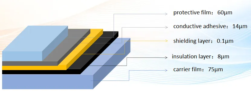
Low-cost shielding components include adhesive copper foils applied post-fabrication. Thin (35 μm) foils conform to irregular surfaces, offering 60-80 dB SE up to 1 GHz at fractions of metal can prices. Conductive paints, sprayed or silk-screened, suit prototypes and low-volume runs. Nickel-graphite formulations balance adhesion and conductivity, curing at room temperature to avoid reflow complications.
Gaskets made from fabric-over-foam provide compressible seals for enclosure joints, outperforming rigid clips in vibration-prone environments. Economical electronic manufacturing favors selective shielding, targeting hotspots like clock generators or RF amplifiers. Partial cans over critical ICs minimize material use while achieving localized SE exceeding 50 dB.
Hybrid approaches combine layout with ferrimagnetic sheets. Thin absorbers (0.1-0.5 mm) suppress cavity resonances in enclosures, enhancing overall performance cost-neutrally.
Best Practices for Implementation in Manufacturing
Begin with simulation-driven design, modeling fields via Maxwell equations to predict weak points. Tools assess plane splits and trace routing impacts, optimizing before prototyping. Factory insights emphasize via density; excessive counts inflate drill costs, so space judiciously per frequency needs.
Material qualification per IPC-6012 ensures plating integrity for ground connections. Avoid blind vias unless essential, as they raise expenses. Assembly processes benefit from fiducials aligning foil overlays precisely.
Testing validates efficacy using near-field probes or reverberation chambers, correlating to IEC radiated immunity levels. Iterative shielding refines based on emissions spectra, prioritizing budget-friendly RF shielding solutions like tape over full enclosures.
Procurement teams source bulk foils and paints, negotiating for volume discounts. Sustainability angles favor recyclable aluminum over exotics. Maintenance protocols include post-assembly inspections for delamination.
Multidisciplinary reviews integrate mechanical constraints, ensuring shields withstand thermal cycling without warping.
Case Insights from Manufacturing Floors
In high-volume runs, transitioning to four-layer boards with dual ground planes cut EMI failures by half, per internal audits. One scenario involved RF modules where via fencing replaced $2-per-unit cans, saving 30% on shielding costs. Performance held at 40 dB isolation up to 2.4 GHz.
Troubleshooting common issues like ground loops reveals discontinuity fixes via capacitors. Factory-driven adjustments, such as edge plating, enhance continuity affordably.
Conclusion
Cost-effective EMI shielding harmonizes performance and budget through smart design and economical materials. Ground planes, via fences, and foils deliver robust protection without extravagance. Electric engineers armed with these strategies optimize economical electronic manufacturing. Prioritizing standards and testing ensures reliability across lifecycles.
FAQs
Q1: What are the most cost-effective EMI shielding techniques for PCBs?
A1: Cost-effective EMI shielding relies on solid ground planes and via stitching to create low-impedance barriers, attenuating noise across RF bands. These affordable PCB shielding methods integrate seamlessly during fabrication, minimizing add-on costs. Selective copper foils provide targeted protection for hotspots, balancing SE with material savings. Implementation per design guidelines yields 30-50 dB isolation economically.
Q2: How do low-cost shielding components impact manufacturing budgets?
A2: Low-cost shielding components like adhesive foils and conductive paints reduce expenses by avoiding custom metalwork, suitable for high-volume runs. They maintain performance in budget-friendly RF shielding solutions while simplifying assembly. Factory processes handle application via standard printing, cutting labor. Trade-offs include lower long-term durability, offset by volume pricing.
Q3: What role does PCB layout play in affordable shielding?
A3: PCB layout optimizes affordable PCB shielding methods through minimized loop areas and guard traces, suppressing crosstalk inherently. Ground plane continuity per IPC-2221 prevents resonances, enhancing isolation without extras. Engineers route high-speed lines internally, leveraging multilayer shielding. This proactive approach trims component budgets significantly.
Q4: Can economical electronic manufacturing achieve high RF shielding performance?
A4: Economical electronic manufacturing attains high RF shielding via hybrid techniques like absorbers over ground planes, targeting cavity modes effectively. Compliance with IEC standards verifies attenuation without premiums. Selective application focuses resources, delivering 60 dB SE where needed. Scalable processes ensure cost stability across volumes.
References
IPC-2221B — Generic Standard on Printed Board Design. IPC, 2003
IPC-6012E — Qualification and Performance Specification for Rigid Printed Boards. IPC, 2015
IEC 61000-4-3 — Electromagnetic Compatibility (EMC) — Part 4-3: Testing and Measurement Techniques — Radiated, Radio-Frequency, Electromagnetic Field Immunity Test. IEC, 2020


