Introduction
Crystal oscillators serve as the precise heartbeat for countless electronic circuits on printed circuit boards (PCBs). These compact components generate stable clock signals essential for synchronizing digital logic, microcontrollers, and communication interfaces. Without their reliability, modern devices from consumer gadgets to industrial controls would falter under timing inconsistencies. In PCB design, crystal oscillators often go unnoticed amid flashier elements like processors, yet their role in ensuring frequency accuracy is irreplaceable. This deep dive explores crystal oscillator basics, their working principle, advantages, applications in PCBs, and frequency stability factors that engineers must consider for robust designs.
Crystal Oscillator Basics: Understanding the Fundamentals
A crystal oscillator relies on a quartz crystal resonator cut to specific dimensions to vibrate at a precise frequency. Quartz exhibits the piezoelectric effect, where mechanical stress generates an electric charge, and an applied voltage induces mechanical deformation. The crystal acts as a high-Q bandpass filter in an oscillator circuit, selecting a single resonant frequency from the amplifier's feedback loop. Engineers specify crystals by fundamental frequency, typically from 1 MHz to 50 MHz for PCB applications, along with load capacitance and tolerance ratings. These parameters directly influence PCB layout decisions, such as trace lengths and grounding to minimize parasitic effects. Crystal oscillator basics form the foundation for any timing-critical design, demanding attention to environmental factors like temperature and shock.
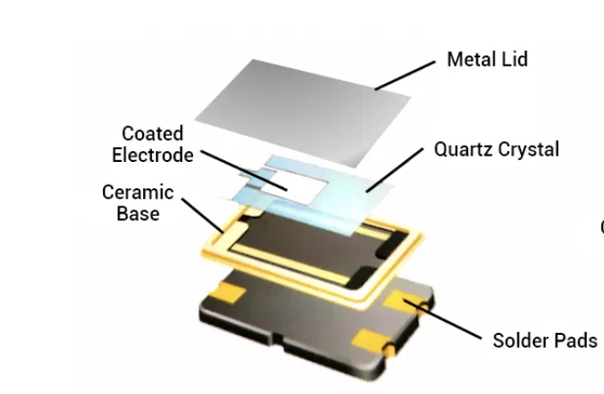
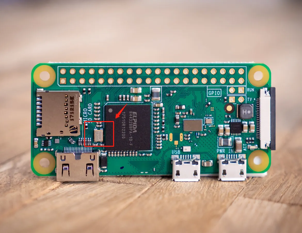
Common types include fundamental mode crystals for lower frequencies and overtone modes for higher ones, each with trade-offs in power consumption and stability. Surface-mount packages like HC-49 or SMD variants dominate modern PCBs for their compact footprint and automated assembly compatibility. Selecting the right crystal involves balancing cost, size, and performance specs against application needs. Neglecting these basics can lead to startup failures or drift in long-term operation.
Crystal Oscillator Working Principle: Piezoelectric Precision in Action
The crystal oscillator working principle centers on positive feedback in an amplifier circuit sustaining crystal vibrations. In a typical Pierce oscillator topology, the crystal connects between the inverter gate and a feedback capacitor network to ground. The amplifier provides 180-degree phase shift, and the crystal adds another 180 degrees at resonance, creating the full 360-degree loop for oscillation. Load capacitors, usually 10-30 pF each, tune the circuit to the crystal's specified parallel resonance mode. Startup occurs when noise triggers the crystal into its stable mode, typically within milliseconds.
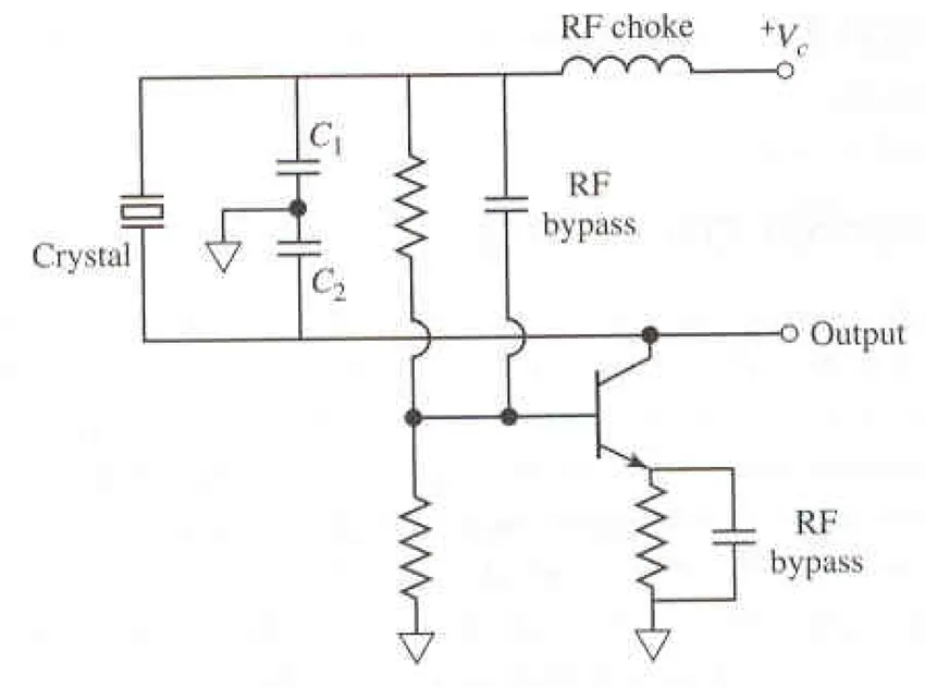
Equivalent circuit models represent the crystal as a series RLC branch shunted by parallel capacitance, where motional resistance determines drive level. Excessive drive current can cause mode jumping or crystal aging, so engineers limit it via resistor values. Temperature variations shift resonance due to quartz's turnover temperature curve, often optimized near 25°C. Understanding this principle guides PCB trace routing to avoid coupling with adjacent signals.
Crystal Oscillator Frequency Stability: Key Factors for Reliable Performance
Crystal oscillator frequency stability measures how well the output holds against variations in temperature, voltage, aging, and load. Stability is quantified in parts per million (ppm), with typical values from ±10 ppm for commercial to ±0.5 ppm for precision units. Temperature coefficient follows an S-curve, with AT-cut crystals minimizing deviation around room temperature. Engineers select crystals with specified aging rates, often under 1 ppm per year, to ensure long-term accuracy in PCBs.
Load capacitance mismatch causes pulling, shifting frequency by up to 10-20 ppm, so PCB stray capacitance must match datasheet values precisely. Voltage sensitivity, or g-sensitivity under vibration, affects high-reliability applications like aerospace. Following IPC-7351 guidelines for land pattern design helps maintain consistent capacitance. Stability testing involves environmental chambers to verify performance across operating ranges.
Crystal Oscillator Advantages: Why They Outshine Alternatives
Crystal oscillators offer superior frequency stability compared to RC or ceramic resonators, making them ideal for precision timing. Their high quality factor (Q > 10,000) results in low phase noise, crucial for RF and data recovery circuits. Power efficiency suits battery-operated devices, with standby currents below 1 μA in some low-power variants. Unlike voltage-controlled oscillators, crystals provide inherent pullability for fine-tuning via varactors.
Key advantages include:
- Exceptional long-term stability with minimal drift over years.
- Compact size fitting dense PCB layouts.
- Wide temperature range options from -40°C to 125°C.
- Cost-effective for high-volume production.
These traits position crystal oscillators as the go-to for applications demanding reliability. In contrast, MEMS oscillators, while rugged, often lag in phase noise for high-end uses.
Crystal Oscillator Applications in PCBs: From Clocks to Communications
Crystal oscillator applications in PCBs span microcontrollers needing 32.768 kHz watch crystals for real-time clocks to 25 MHz references for Ethernet PHYs. In wireless modules, they clock transceivers for Wi-Fi or Bluetooth, ensuring carrier frequency accuracy. Automotive ECUs rely on them for CAN bus timing, enduring harsh vibrations per AEC-Q100 qualification. Industrial PLCs use dual crystals for redundancy in safety-critical systems.
Servers and routers employ Oven-Controlled Crystal Oscillators (OCXOs) for stratum-1 timing, achieving ppb stability. In power supplies, crystals synchronize switchers to reduce EMI. PCB integration demands isolated routing and via stitching for shielding. J-STD-001 soldering standards ensure reliable joints, preventing micro-cracks from thermal cycling.
Best Practices for Crystal Oscillator Integration on PCBs
Place crystals close to the load IC, within 20 mm, to minimize trace inductance. Use ground planes under the crystal footprint, avoiding splits that introduce noise. Select load capacitors as 0402 or smaller SMD types with low ESR for high frequencies. Simulate startup time using SPICE models to verify margin.
Decoupling capacitors near power pins suppress supply noise, targeting <50 mV ripple. Guard traces around crystal lines shield from crosstalk. Bake crystals before assembly if exposed to humidity, aligning with JEDEC J-STD-033 handling. Thermal vias dissipate heat in high-drive setups. These practices enhance yield and field reliability.
Troubleshooting Crystal Oscillator Issues: Practical Engineering Fixes
Failure to oscillate often stems from incorrect load capacitance; measure with a grid dip meter or scope. High phase noise indicates drive level excess, addressed by adding series resistor. Frequency drift points to temperature effects or aging; verify turnover point matches environment. Intermittent startup in cold conditions requires higher drive or parallel mode selection.
Vibration sensitivity in mobile devices calls for stress-relieved mounting per IPC guidelines. Scope probing adds capacitance, falsifying measurements, so use ×10 probes. Logic analyzer captures reveal clock glitches from PDN noise. Systematic debugging restores timing integrity.
Conclusion
Crystal oscillators remain indispensable for PCB timing, delivering unmatched stability and precision. Mastering their basics, working principle, advantages, applications, and frequency stability empowers engineers to build resilient designs. By adhering to layout best practices and standards, common pitfalls become avoidable. As PCB densities rise, these unsung heroes will continue underpinning technological progress.
FAQs
Q1: What are the crystal oscillator basics for PCB designers?
A1: Crystal oscillator basics involve a quartz resonator in a feedback loop generating stable frequencies via piezoelectricity. Key specs include frequency, load capacitance, and stability in ppm. On PCBs, they provide clock signals for MCUs and interfaces, outperforming RC types in accuracy. Proper selection ensures reliable startup and minimal drift.
Q2: How does the crystal oscillator working principle ensure precision?
A2: The crystal oscillator working principle uses the quartz crystal's high-Q resonance in a Pierce circuit for self-sustaining oscillation. Feedback capacitors tune to parallel mode, locking frequency tightly. This yields low phase noise and high stability, vital for digital synchronization. Environmental factors like temperature influence performance, requiring spec-matched layouts.
Q3: What are the main crystal oscillator advantages over other timing sources?
A3: Crystal oscillator advantages include superior frequency stability, low phase noise, and compact form for dense PCBs. They offer ppm accuracy across temperatures, unlike ceramic resonators prone to drift. Power efficiency suits portables, and cost scales well for volume. These traits make them essential for comms and control applications.
Q4: Why is crystal oscillator frequency stability critical in PCB applications?
A4: Crystal oscillator frequency stability, measured in ppm, prevents timing errors in microcontrollers, RF modules, and networks. Factors like temperature, load mismatch, and aging affect it, demanding precise PCB design. Standards like IPC-7351 guide land patterns for optimal capacitance. High stability ensures compliance in automotive and telecom PCBs.
References
IPC-7351C — Generic Requirements for Surface Mount Design and Land Pattern Standard. IPC, 2010
J-STD-001H — Requirements for Soldered Electrical and Electronic Assemblies. IPC/JEDEC, 2020
JEDEC J-STD-033D.1 — Handling, Packing, Shipping, and Use of Moisture/Reflow Sensitive Surface Mount Devices. JEDEC, 2018


