Introduction
Functional testing stands as a critical final step in PCB prototype validation, ensuring that the assembled board performs its intended functions under realistic operating conditions. Electric engineers rely on this method to bridge the gap between individual component verification and full system integration, catching issues that earlier PCB testing methods might overlook. By simulating end-user scenarios, functional testing confirms signal integrity, power distribution, and interconnectivity across the prototype. This process minimizes risks before scaling to production, aligning with quality expectations in demanding applications. Among various PCB testing methods, functional testing provides the most comprehensive validation, complementing techniques like in-circuit testing (ICT). Mastering functional test development and test fixture design empowers engineers to deliver reliable prototypes efficiently.
Why Functional Testing Matters in Prototype Development
Prototype validation demands more than bare board checks or assembly inspections; it requires proof that the PCB operates as a cohesive unit. Functional testing verifies that all subsystems interact correctly, from power-on self-tests to data processing outputs. Unlike preliminary scans, this approach exposes timing errors, firmware incompatibilities, and thermal effects that only emerge in operation. In the PCB lifecycle, skipping thorough functional testing can lead to costly redesigns or field failures, eroding trust in the prototype. Engineers prioritize it to meet performance specs, ensuring compliance with assembly standards like IPC-A-610 for acceptability criteria. Ultimately, robust functional testing accelerates time-to-market while upholding reliability.
Overview of Key PCB Testing Methods
PCB testing methods form a layered strategy, starting with visual and automated optical inspections, progressing to electrical continuity checks, and culminating in functional validation. In-circuit testing (ICT) uses a bed-of-nails fixture to probe thousands of points, measuring resistance, capacitance, and shorts on assembled boards. This method excels at component-level faults but falls short on board-level interactions. Flying probe testers offer flexibility for low-volume prototypes, moving probes dynamically without custom fixtures. Functional testing, however, integrates all prior checks by applying inputs and observing outputs, mimicking real-world use. Selecting the right combination depends on prototype complexity, board density, and test coverage goals.
In-Circuit Testing (ICT): A Foundation for Functional Validation
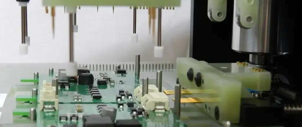
In-circuit testing (ICT) provides high-resolution data on individual components and nets, serving as a prerequisite for functional test development. Engineers press the prototype into a custom fixture where spring-loaded probes contact test points, enabling automated measurements of voltage levels, diode drops, and passive values. ICT detects assembly defects like solder bridges or missing parts early, achieving test coverage above 90% for accessible nodes. Limitations arise with densely packed boards or guarded components, where access probes may interfere. Despite these, ICT remains essential, feeding diagnostic data into functional setups. Integrating ICT results streamlines prototype validation by isolating issues before full-system tests.
Principles of Functional Test Development
Functional test development begins with a detailed requirements analysis, mapping design schematics to expected behaviors under power and signals. Engineers define test vectors: sequences of inputs like digital patterns, analog voltages, or communication protocols that trigger board responses. Software tools generate these vectors, simulating microcontroller code or sensor interfaces without full enclosure integration. Test coverage metrics ensure critical paths, from power rails to high-speed buses, receive validation. Incorporating boundary scan (JTAG) enhances accessibility for embedded logic. This structured approach aligns functional tests with prototype specs, reducing false positives through iterative refinement.
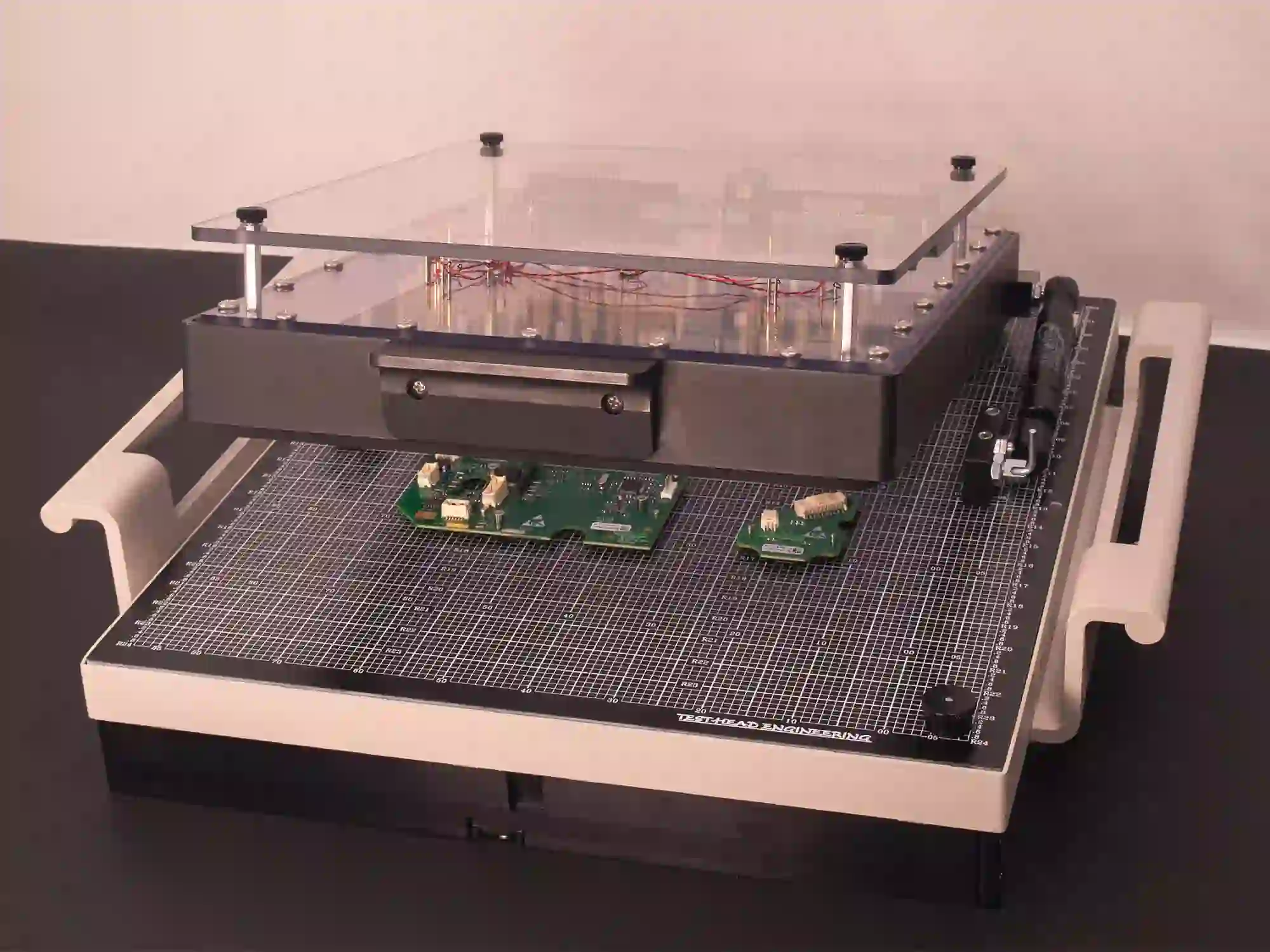
Designing Effective Test Fixtures
Test fixture design directly impacts test repeatability and accuracy, requiring mechanical precision to interface reliably with the PCB prototype. Engineers select materials like phenolic or aluminum for the base, ensuring planarity within tolerances for uniform probe contact. Probe placement follows design files, spacing pogo pins 0.1 inches apart minimum to avoid crosstalk, with force calibrated at 1-2 ounces per probe. Vacuum hold-down secures the board, while interposers handle connectors or edge interfaces. For high-density prototypes, hybrid fixtures combine mechanical probes with wireless or edge-card connections. Best practices include design reviews for probe accessibility and modular construction for future revisions.
Implementing Functional Tests Step-by-Step
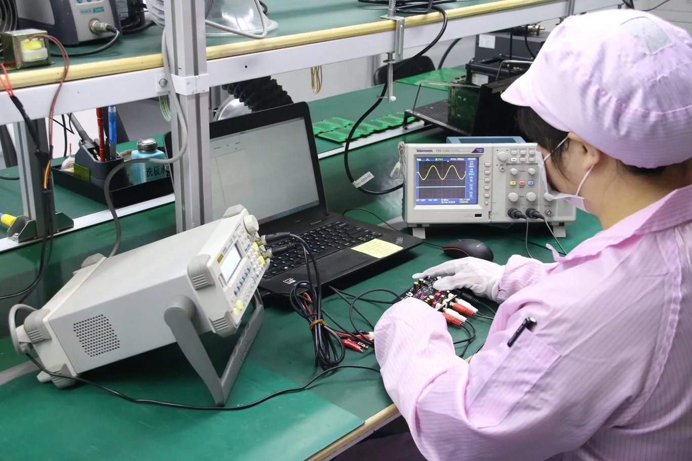
Start functional testing by powering the prototype in a controlled environment, monitoring current draw against expected profiles to flag shorts or leaks. Apply stimulus via the fixture: toggle GPIOs, sweep frequencies, or inject serial data, capturing outputs with scopes or logic analyzers. Software scripts automate pass/fail criteria, logging waveforms for root-cause analysis on failures. Environmental stressors like temperature ramps reveal marginal designs, per guidelines in standards such as J-STD-001 for soldered assemblies. Iterate by tweaking firmware or rerouting traces based on data. Comprehensive logging ensures traceability, supporting design handoff to manufacturing.
Integrating ICT and Functional Testing for Optimal Coverage
Combining in-circuit testing (ICT) with functional methods maximizes prototype validation efficiency. ICT pinpoints assembly flaws, allowing engineers to focus functional tests on system-level verification. Shared fixtures reduce setup time, with ICT probes repurposed for power/ground references in functional runs. Data fusion from both reveals correlations, like a passing ICT net failing under load due to thermal drift. This hybrid strategy achieves near-100% fault coverage for prototypes. Engineers document integration in test plans, ensuring scalability.
Best Practices for Prototype Validation
Adhere to design-for-test (DFT) principles early, allocating test points at vias and adding boundary scan chains. Collaborate between design and test teams to align on metrics like fault grading and escape rates. Calibrate equipment regularly, verifying fixture alignment with golden boards. Employ statistical process control on test yields to predict production issues. Document anomalies with photos and measurements for feedback loops. These practices elevate PCB testing methods from reactive to proactive.
Common Challenges in Functional Testing and Solutions
High-speed signals often challenge functional test development, where crosstalk or impedance mismatches distort results. Mitigate by using controlled-impedance probes and shielding in fixtures. Firmware bugs mimic hardware faults; debug with in-system programmers during tests. Multi-layer boards complicate access, resolved via flying probes or wireless telemetry for inaccessible nodes. Yield variability from hand-assembly demands statistical sampling before full runs. Addressing these systematically ensures reliable prototype validation.
Advanced Considerations for Complex Prototypes
For RF or mixed-signal prototypes, functional tests incorporate spectrum analyzers to validate frequency response and noise floors. Power integrity checks simulate load transients, measuring ripple with high-bandwidth scopes. Thermal imaging spots hotspots during operation, guiding heatsink integration. Compliance with IPC-9252 for electrical test baselines informs functional thresholds. Engineers scale tests via cloud-based emulation for virtual validation pre-fixture build.
Conclusion
Functional testing validates PCB prototypes comprehensively, confirming design intent through real-world simulation. Key PCB testing methods like in-circuit testing (ICT) lay groundwork, while thoughtful functional test development and test fixture design ensure precision. Electric engineers benefit from standard-aligned practices, minimizing risks and accelerating iterations. Prioritizing this stage upholds quality from prototype to production. Invest in robust strategies to achieve dependable outcomes.
FAQs
Q1: What are the main differences between ICT and functional testing in PCB validation?
A1: In-circuit testing (ICT) focuses on component-level electrical measurements using fixed probes for continuity and values, ideal for assembly defects. Functional testing simulates operational conditions, verifying interactions and outputs across the board. ICT offers high node coverage but misses system issues; functional provides holistic prototype validation. Combine both for complete fault detection.
Q2: How do you develop a functional test for a PCB prototype?
A2: Functional test development starts with spec review, creating input vectors from schematics and firmware. Define pass/fail limits for signals, power, and timings. Use automated scripts on test fixtures to run sequences repeatedly. Incorporate DFT features like JTAG for deeper access. Refine based on failures for optimal coverage.
Q3: What factors influence test fixture design for PCB testing methods?
A3: Test fixture design considers board size, probe count, and access points, using precise pogo pins for contact. Material choice affects durability, while vacuum secures alignment. Account for connectors and environmental needs. Modular designs support revisions. Proper spacing prevents shorts, ensuring reliable prototype validation.
Q4: Why is prototype validation critical before PCB production?
A4: Prototype validation via functional testing catches design flaws early, avoiding expensive production runs. It verifies performance under load, aligning with standards like IPC-A-610. Reduces field failures and iterations. Ensures scalability and compliance.
References
IPC-A-610H — Acceptability of Electronic Assemblies. IPC, 2019
IPC-9252B — Requirements for Electrical Testing of Unpopulated Printed Boards. IPC, 2016
J-STD-001G — Requirements for Soldered Electrical and Electronic Assemblies. IPC, 2017


