Introduction
Hall effect current sensors provide a reliable method for non-contact current measurement in power electronics applications, such as motor drives, inverters, and battery management systems. These sensors detect the magnetic field generated by current flowing through a conductor, offering galvanic isolation between the high-current path and the sensing circuitry. In PCB layouts, optimal hall effect sensor pcb placement is critical to minimize stray magnetic field interference, which can degrade hall effect sensor accuracy. Coreless current sensor designs, popular for their compact size and low profile, are particularly susceptible to external magnetic noise from nearby traces, inductors, or switching components. Poor placement leads to offset errors, reduced linearity, and compromised pcb current sensor isolation performance. Engineers must prioritize layout strategies that enhance noise immunity while adhering to established design principles.
This article explores the technical underpinnings of noise in these sensors and delivers structured best practices for PCB design. By understanding magnetic field interactions, designers can achieve precise measurements even in noisy environments. Key considerations include conductor orientation, ground plane management, and separation from interference sources. These approaches ensure robust performance across operating conditions. Ultimately, thoughtful hall effect sensor pcb placement transforms potential vulnerabilities into strengths for reliable system operation.
What Are Hall Effect Current Sensors and Why Does Placement Matter?
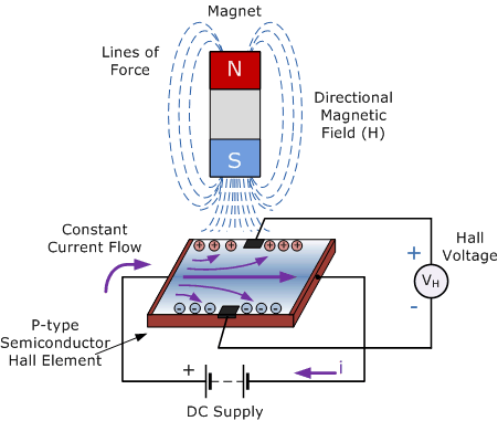
Hall effect current sensors operate on the Hall principle, where a voltage is generated across a conductor perpendicular to both current flow and an applied magnetic field. In current sensing, the sensor element sits adjacent to a current-carrying trace or busbar, converting the produced magnetic field into a proportional output voltage or current. Coreless variants eliminate ferromagnetic cores, reducing size and hysteresis but increasing sensitivity to ambient fields. Pcb current sensor isolation is a primary advantage, as the sensor provides electrical separation up to several kilovolts, essential for safety in high-voltage systems.
Placement matters because stray magnetic field interference from parallel currents, ground returns, or power devices induces unwanted offsets in the sensor output. In multi-phase systems, fields from adjacent phases couple directly into the sensor, causing crosstalk and measurement errors up to several percent. Hall effect sensor accuracy, often specified below 1% over temperature, degrades without proper layout isolation. Compact PCB designs exacerbate this, as high-current paths and control circuitry share limited board real estate. Optimizing placement aligns the primary field while rejecting common-mode noise, preserving linearity and bandwidth.
Following IPC-2221B guidelines for trace routing and spacing helps mitigate these risks by promoting controlled signal integrity. Designers targeting electric vehicle inverters or renewable energy converters cannot afford compromised sensing, where even minor inaccuracies cascade into control loop instabilities. Strategic positioning ensures the sensor captures the intended differential field while nullifying homogeneous external influences.
Technical Principles of Stray Magnetic Field Interference
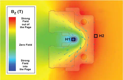
Stray magnetic fields arise from any current path on the PCB, looping according to Ampere's law and penetrating the Hall plate. In coreless current sensors, the small die size amplifies the effect of nearby fields, as there is no flux concentration to discriminate the target signal. Common sources include return paths under the sensor, adjacent power traces, and eddy currents in ground planes. These induce a uniform bias field, shifting the null point and introducing nonlinearity proportional to the interfering current magnitude.
The sensor's common-mode rejection relies on differential Hall elements arranged to cancel symmetric fields. However, asymmetric layouts disrupt this balance, leading to residual sensitivity. For instance, a ground plane on the opposite layer creates opposing loops that partially cancel but introduce temperature-dependent drifts. Frequency-domain effects compound issues, as switching noise from MOSFETs generates high-frequency fields that couple capacitively or magnetically.
Coreless designs excel in high-bandwidth applications but demand precise field modeling during layout. Finite element simulations reveal hotspots where stray fields peak, guiding iterative refinements. Pcb current sensor isolation extends to magnetic domains, requiring barriers like slots or mu-metal shields in extreme cases, though these add complexity.
Bandwidth limitations stem from internal compensation loops, typically 100 kHz to 1 MHz, making layout immunity vital for capturing transients without aliasing.
Best Practices for Optimizing Hall Effect Sensor PCB Placement
Position the sensor directly above or below the primary current trace, centered for maximum coupling, with the Hall plate plane parallel to the trace for optimal sensitivity. Orient the current conductor perpendicular to the PCB plane when possible, routing it via vias to inner layers, allowing flux lines to loop vertically through the sensor. Maintain at least 5 times the trace width separation from parallel high-current paths to reduce gradient-induced errors. Slot the ground plane under the sensor to break eddy current loops, optimizing pcb current sensor isolation without compromising thermal performance.
Implement symmetric ground pours around the sensor, balancing copper on all sides to minimize offset from thermal expansion mismatches. Use multi-layer boards with dedicated sensing layers, shielding noisy power planes above and below. For coreless current sensors, follow ground plane cutouts as per application notes, tapering edges to avoid field fringing. Decouple the sensor supply with 0.1 μF ceramics placed within 2 mm, and route analog outputs differentially over short paths to the ADC.
Adhering to IPC-7351C land pattern standards ensures reliable soldering and minimal parasitics during assembly. In three-phase inverters, stagger sensor placements azimuthally to decorrelate phase fields. Test prototypes with Helmholtz coils to quantify stray rejection, iterating layouts for under 0.5% error.
Guard traces around signal lines reject capacitive noise, while ferrite beads on power inputs suppress conducted EMI. These practices yield robust noise immunity across automotive and industrial grades.
Troubleshooting Common Placement Issues
Engineers often encounter offset drifts traceable to unbalanced ground returns under the sensor. Verify symmetry by probing field homogeneity with a gaussmeter during prototyping. Crosstalk in polyphase systems manifests as ripple at switching harmonics; mitigate by increasing inter-phase spacing or adding phase-specific shields.
Coreless sensors show heightened sensitivity to PCB flexure, inducing piezoresistive offsets. Reinforce mounting areas per J-STD-001 requirements for mechanical stability. Temperature gradients from nearby heatsinks cause calibration shifts; isolate thermally with slots or low-k dielectrics.
Field mapping tools reveal hidden interferers like via farms; reroute to periphery. Post-layout simulations validate before fabrication.
Conclusion
Optimizing hall effect sensor pcb placement demands a holistic view of magnetic interactions, from conductor geometry to ground topology. Coreless current sensors offer compelling advantages in size and speed but require vigilant stray magnetic field interference mitigation. By centering sensors on target paths, symmetrizing planes, and distancing noise sources, engineers achieve superior hall effect sensor accuracy and pcb current sensor isolation. Integrating these with IPC standards ensures manufacturability and reliability. Prioritizing layout early prevents costly respins, enabling precise control in demanding applications.
FAQs
Q1: What causes stray magnetic field interference in hall effect sensor pcb placement?
A1: Stray fields originate from nearby current-carrying traces, ground loops, inductors, and switching elements on the PCB. These uniform fields bias the Hall plate, causing output offsets that degrade hall effect sensor accuracy. Symmetric layouts and plane slots cancel common-mode components effectively. Proper separation maintains linearity in coreless designs.
Q2: How does pcb current sensor isolation improve with optimized placement?
A2: Strategic routing orients flux vertically, enhancing differential sensitivity while rejecting lateral strays. Ground plane management prevents eddy coupling, preserving galvanic barriers. This boosts noise immunity without additional components, ideal for high-voltage systems.
Q3: Why are coreless current sensors sensitive to PCB layout?
A3: Without flux concentrators, they rely on ambient field geometry for accuracy. Asymmetries amplify errors from stray magnetic field interference. Tailored ground cutouts and perpendicular conductors optimize performance per design guidelines.
Q4: What IPC standards guide hall effect sensor placement?
A4: IPC-2221B addresses trace spacing and routing for signal integrity. IPC-7351C standardizes land patterns to minimize parasitics. These ensure reliable integration and assembly.
References
IPC-2221B — Generic Standard on Printed Board Design. IPC, 2012
IPC-7351C — Generic Requirements for Surface Mount Design and Land Pattern Standard. IPC, 2014
J-STD-001H — Requirements for Soldered Electrical and Electronic Assemblies. IPC, 2020


