Introduction
In high-voltage PCB applications, such as power inverters, electric vehicle chargers, and industrial motor drives, accurate current measurement is essential for control, protection, and efficiency. Isolated current sensors provide a safe way to monitor currents without direct electrical connection between high-voltage and low-voltage circuits. This galvanic isolation prevents hazardous voltage transfer, ground loops, and noise interference that could compromise system reliability. Designing these sensors into PCBs requires careful attention to isolated current sensor design principles, particularly in high voltage PCB design where safety margins are critical. Engineers must balance performance, compactness, and compliance to ensure robust operation under demanding conditions. Key challenges include maintaining adequate creepage and clearance distances while integrating sensing elements effectively.
What Are Isolated Current Sensors and Why They Matter in High-Voltage PCBs
Isolated current sensors detect current flow in a primary conductor while keeping the measurement circuitry electrically separated from it. Common types include Hall effect sensors, which use magnetic fields to sense current non-invasively, current transformers for AC measurements, Rogowski coils for high-frequency transients, and shunt-based sensors paired with isolation amplifiers. Galvanic isolation ensures no conductive path exists between the high-voltage side and the signal processing side, typically achieving isolation voltages from several kV to tens of kV. In high voltage PCB design, these sensors matter because they protect users and equipment from shock hazards, enable precise feedback for power electronics, and comply with safety regulations.
Failure to implement proper isolation can lead to arcing, insulation breakdown, or false readings that trigger system faults. For electric engineers working on applications exceeding 1 kV, such as renewable energy systems or traction inverters, isolated current sensors enhance signal integrity by rejecting common-mode noise. They also support reinforced isolation requirements, where a single barrier must withstand twice the voltage stress of basic isolation. Ultimately, thoughtful isolated current sensor design extends PCB lifespan and minimizes field failures in harsh environments.
Technical Principles of Galvanic Isolation in Current Sensing
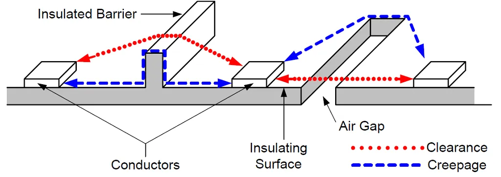
Galvanic isolation in current sensors relies on physical barriers that block direct current flow while allowing signal or magnetic coupling. Magnetic isolation, used in Hall effect and current transformer types, couples flux from the primary current to a secondary winding or sensor core without physical contact. Capacitive isolators transfer signals via electric fields across dielectric layers, suitable for high-speed data from shunts. Optical methods convert electrical signals to light and back, offering excellent isolation but higher power draw. Each method influences PCB layout, as the isolation barrier must span sufficient creepage and clearance distances to prevent partial discharge or flashover.
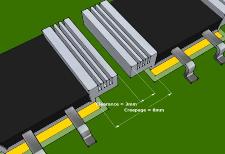
Creepage distance measures the shortest path along the PCB surface between two conductive parts, accounting for contamination and tracking. Clearance, in contrast, is the shortest air path through insulation, critical for arc prevention in dry conditions. These distances scale with working voltage, pollution degree, and material comparative tracking index (CTI). IPC-2221 provides guidelines for calculating external and internal spacings on PCBs, factoring in conductor elevation and coatings. For reinforced isolation, common in safety-critical designs, the barrier must endure higher test voltages, often doubling basic insulation levels.
Pollution degree classifications further refine requirements: degree 1 assumes clean environments, while degree 3 suits industrial dust and moisture. Material group per CTI affects creepage, with group I materials (CTI >600) allowing tighter spacing than group III (CTI 100-400). Engineers must map these principles to PCB stackups, ensuring vias, traces, and components respect both metrics. Reinforced isolation per relevant IEC standards demands coordinated dimensions across the entire barrier.
PCB Layout Challenges and Solutions for Isolated Current Sensors
High voltage PCB design demands strategic component placement to maximize isolation margins. Position the current sensor's primary path centrally, routing high-voltage traces away from low-voltage signal lines with wide slots or guard rings. Slots etched into the PCB increase creepage by forcing surface paths to detour, effectively doubling distances in compact boards. Use multi-layer stackups where inner layers provide additional dielectric separation, but verify internal clearance per IPC-2221 tables adjusted for board thickness.
Component selection plays a key role: choose sensors with integrated isolation rated for the system's peak voltage and common-mode transient immunity. Shunt resistors on the high-voltage side require low-inductance Kelvin connections, isolated via amplifiers with capacitive or magnetic barriers. For Hall effect sensors, align the IPM package perpendicular to the current busbar to optimize flux capture while maintaining clearance. Conformal coatings boost creepage by filling gaps and repelling contaminants, but select types compatible with high CTI bases like FR4-G10 or ceramic-filled laminates.
Guard traces, floated or driven to intermediate potentials, distribute voltage gradients evenly, reducing field stress. Simulate electric fields using finite element analysis to predict hotspots before fabrication. In reinforced isolation setups, segment the PCB with cutouts or potting compounds to create hybrid barriers combining air, solid, and surface paths.
Best Practices for Reliability and Compliance
Adhere to systematic verification: calculate minimum spacings using voltage, altitude derating (1.1% per 300m above 1000m), and overvoltage categories. IEC 60664-1 outlines insulation coordination, including phase-to-phase and working voltages for pollution degrees 1-3. Prototype testing involves hi-pot sweeps up to 5-10 kV, partial discharge checks at operational levels, and impulse withstand per reinforced isolation specs.
Thermal management affects isolation: hotspots accelerate dielectric aging, so integrate heat sinking without bridging barriers. Bandwidth considerations guide type selection; Rogowski coils excel in transients but need integrators, while Hall sensors offer DC accuracy. Multi-sensor redundancy in critical apps enhances fault tolerance.
Document design rationale with stackup drawings, spacing audits, and material datasheets for certification. Collaborate early with fabrication partners versed in high-voltage processes like controlled depth routing for slots.
(Insert image: 'High-Voltage Testing Setup for Isolation' · ALT: 'Engineer performing hi-pot test on PCB with isolated current sensor')
Troubleshooting Common Issues in High-Voltage Implementations
Engineers often encounter arcing from overlooked pollution buildup, resolved by uprating creepage 20-50% for degree 2 environments. Noise coupling through parasitic capacitance plagues capacitive isolators; mitigate with ground planes shielding low-side signals. Bandwidth droop in CTs at low currents necessitates bias currents or Hall hybrids.
In one typical scenario for a 1.2 kV inverter PCB, initial prototypes failed hi-pot due to via proximity; redesigning with staggered vias and filled slots passed reinforced isolation tests. Moisture ingress post-assembly caused tracking; conformal coating per IPC class H resolved it. Systematic DFMEA identifies such risks upfront.
Conclusion
Isolated current sensor design in high-voltage PCB applications hinges on mastering galvanic isolation, creepage and clearance, and reinforced isolation principles. Logical layout, material choices, and standards compliance ensure safety and performance. Electric engineers benefit from structured approaches like slotting, guards, and simulations to navigate these challenges. Prioritizing these considerations yields reliable systems ready for demanding fields. Future trends toward higher voltages underscore the need for ongoing adherence to evolving guidelines.
FAQs
Q1: What factors determine creepage and clearance in isolated current sensor design?
A1: Creepage follows surface paths influenced by CTI material group and pollution degree, while clearance measures air gaps based on peak voltage. High voltage PCB design requires consulting IPC-2221 for external spacings and derating for altitude. Reinforced isolation doubles these for safety. Always verify with simulations to account for component geometry and coatings. [1] [2]
Q2: How does galvanic isolation enhance high voltage PCB design reliability?
A2: Galvanic isolation blocks DC and low-frequency AC paths, preventing shocks and noise in current sensing. Methods like magnetic coupling in Hall sensors suit PCB integration. It supports reinforced isolation per IEC standards, vital for power electronics. Proper implementation avoids ground loops and ensures signal fidelity across barriers. [3]
Q3: Why prioritize reinforced isolation in isolated current sensor applications?
A3: Reinforced isolation provides a single robust barrier equivalent to double insulation, mandatory for patient proximity or hazardous locations. In high voltage PCB design, it withstands higher transients per IEC 62368-1. This simplifies certification while maximizing creepage efficiency. Engineers calculate spacings accordingly for compliance. [3]
Q4: What PCB techniques improve creepage in high-voltage current sensing?
A4: Etch slots, apply conformal coatings, and use high-CTI substrates to extend surface paths. Guard rings equalize potentials, reducing stress. Align traces to minimize bends where contamination accumulates. These align with IPC-2221 for reliable galvanic isolation in compact designs. [4]
References
IPC-2221B — Generic Standard on Printed Board Design. IPC
IEC 60664-1 — Insulation Coordination for Equipment within Low-Voltage Systems. IEC
IEC 62368-1 — Audio/Video, Information and Communication Technology Equipment. IEC


