Introduction
Through-hole technology remains a cornerstone in PCB assembly, particularly for mixed-technology boards that combine THT components with surface-mount devices. Electrical engineers often encounter scenarios where high-reliability connectors, power transistors, or heat sinks demand the mechanical strength of through-hole assembly. In batch production, mastering wave soldering for THT components ensures efficiency while maintaining joint integrity amid the complexities of mixed technology assembly. This process integrates seamlessly after surface-mount reflow, allowing high-volume throughput without compromising quality. Understanding these dynamics helps engineers optimize designs for manufacturability and troubleshoot assembly issues effectively. As demands for hybrid PCBs grow, proficiency in THT wave soldering becomes essential for reliable PCB manufacturing processes.
What Is Through-Hole Technology and Why It Matters in Mixed-Technology PCBs
Through-hole technology involves inserting component leads through drilled holes in the PCB, securing them mechanically before soldering. This contrasts with surface-mount technology, where components sit directly on pads, enabling denser layouts but less robustness for certain applications. THT components excel in environments requiring vibration resistance, high current handling, or easy rework, such as in industrial controls or power supplies. In mixed technology assembly, THT complements SMT by handling bulky parts that SMT cannot accommodate reliably. Engineers value this hybrid approach for balancing density with durability in compact designs. Batch assembly leverages THT's suitability for automated insertion and wave soldering, streamlining production for medium to high volumes.
The relevance of through-hole assembly persists despite SMT dominance, as many legacy and high-power designs mandate it. Standards like IPC J-STD-001 outline requirements for soldered joints, ensuring consistency across classes from general consumer to high-reliability aerospace. Mixed-technology PCBs benefit from THT's ability to form strong inter-layer connections via plated through-holes. Without proper THT integration, assemblies risk mechanical failures under thermal cycling or mechanical stress. Electrical engineers must consider these factors early in design to avoid costly rework during the PCB manufacturing process.
The Fundamentals of Wave Soldering in Through-Hole Assembly
Wave soldering forms the backbone of THT batch assembly, where boards pass over a molten solder wave for simultaneous joint formation. This inline method, which far surpasses hand soldering for consistency in high-volume production, is a core component of the definitive guide to PCB soldering methodologies, standards, techniques, and strategic implementation. The process begins with flux application to remove oxides, followed by preheating to minimize thermal shock before the board contacts the solder pot.
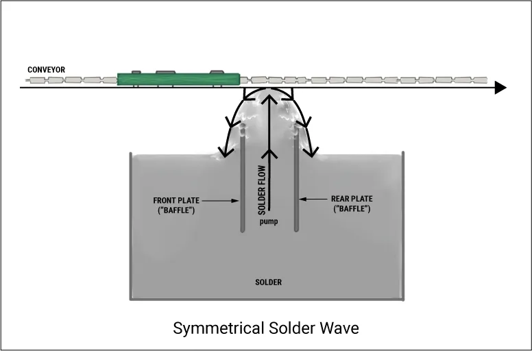
Flux selection proves critical, with no-clean or low-residue types preferred to reduce post-cleaning needs. Engineers troubleshoot flux issues by verifying spray patterns and dwell times, preventing dewetting on copper surfaces. Solder alloy choice, typically Sn63Pb37 or lead-free SAC305, aligns with RoHS compliance and joint reliability. Conveyor angle and speed control contact time, influencing hole fill percentage. Proper fixturing prevents board warpage, especially in mixed-technology boards with asymmetric component loading. Adhering to these principles yields defect rates below 1% in optimized lines.
Technical Principles Behind Effective THT Wave Soldering
The physics of wave soldering relies on capillary action and surface tension to draw solder into through-holes. Flux acids clean pads and leads instantaneously upon heating, while activators ensure barrel wetting up to 75-100% as per industry benchmarks. Preheat temperatures, often 100-150°C, expand materials uniformly and drive off volatiles without delaminating the laminate. The solder pot maintains 250-260°C for eutectic alloys, with laminar flow waves minimizing turbulence that causes bridging. Post-wave cooling at controlled rates prevents brittle intermetallics or cracks from rapid contraction. Electrical engineers analyze these interactions using thermal profiling to predict joint microstructure.
In mixed technology assembly, sequencing matters: SMT reflow precedes THT wave to avoid disturbing fine-pitch parts. Masking or palletizing protects reflowed SMT joints from flux splatter and secondary heating. Shadowing occurs when tall THT components block solder flow to adjacent holes, demanding strategic placement. Hole-to-lead ratios, ideally 0.6-0.8, optimize fill without excess solder balls. Vibration during cooling aids dross removal, enhancing surface finish. Mastering these mechanisms reduces voids and ensures compliance with visual criteria.
Challenges in Mixed-Technology PCB Batch Assembly
Mixed-technology boards introduce thermal mismatches, as SMT components endure two heat exposures: reflow at 220-260°C followed by wave soldering preheat. This risks tombstoning in low-mass SMT parts or degradation of temperature-sensitive polymers. Flux residue on SMT can cause electrochemical migration if not managed, complicating no-clean processes. Component density amplifies bridging risks, where solder bridges span narrow pitches during wave contact. Board size variations demand custom pallets to maintain parallelism over the solder wave. Engineers face these hurdles in high-mix production, where setup times impact throughput.
Plated through-hole reliability under dual processes requires robust copper plating thickness, typically 20-25 microns per IPC guidelines. Solder mask damage from flux pooling erodes insulation resistance over time. Inspection challenges arise from hidden joints, necessitating X-ray or cross-sectioning for verification. Process windows narrow with lead-free solders, demanding precise nitrogen atmospheres to suppress oxidation. Troubleshooting demands root-cause analysis, from design files to inline AOI data. Proactive simulation of thermal profiles mitigates most issues before production.
Best Practices for Through-Hole Assembly in Batch Production
Optimize design with IPC-7251 land patterns, ensuring annular rings support fillet formation without wicking up leads. Component leads should protrude 1-2 mm beyond the board for inspectability and stress relief. Automate insertion using radial or axial machines for repeatability, minimizing bend variations. Flux quantity control via spray volume and board speed prevents over-application that leads to icicles. Preheat profiles ramp gradually to 120°C peak, verified by thermocouples at multiple zones. Solder wave height sets to 70% of board thickness for optimal immersion without flooding.
For mixed technology assembly, employ selective pallets channeling flux and solder only to THT sides. Nitrogen blanketing reduces dross and improves wetting on oxidized surfaces. Inline monitoring of solder chemistry maintains alloy purity above 99%. Post-solder cleaning uses deionized water sprays if residues persist, followed by baking to zero moisture. Inspection per IPC-A-610 criteria flags defects like cold joints or insufficient hole fill early. Engineers refine processes iteratively, targeting Cpk >1.33 for critical parameters.
Process controls extend to drag soldering for double-sided THT, where bottom-side joints reflow during top-side wave. Fixtures with ventilation holes prevent trapped vapors from lifting components. Operator training on J-STD-001 soldering requirements ensures class 2 or 3 compliance. Data logging conveyor speed, temperatures, and defect rates enables SPC analysis. Integrating these practices cuts rework by 50% in mature lines. Continuous improvement aligns with ISO quality systems for sustained yield gains.
Troubleshooting Common Issues in THT Wave Soldering
Bridging tops the defect list, often from excessive solder volume or poor hole alignment. Reduce by adjusting wave height and adding anti-bridge gaps in masks. Insufficient wetting signals flux exhaustion; refresh applicator nozzles and test pH regularly. Solder balls scatter from turbulent waves, resolved by smoothing pot surfaces and stabilizing conveyor. Component standoff too low causes body contact with molten solder, leading to failures; enforce minimum clearances in insertion tooling. Thermal profiling reveals uneven heating, prompting zone recalibration.
In mixed assemblies, SMT delamination traces to preheat spikes; lower ramp rates and add bottom-side cooling. Icicles form from slow drainage, countered by tilting boards post-wave. Voiding in barrels stems from flux entrapment; switch to low-solids formulations. Electrical testing post-assembly pinpoints opens from lead deformation during insertion. Root-cause teams correlate defects to specific lots, refining supplier specs. Proactive measures like daily pot skimming maintain process stability. (Insert image: 'Wave Soldering Defects Examples' · ALT: 'Photographs of common THT defects like bridging, icicles, and poor wetting')
Conclusion
Mastering through-hole technology in mixed-technology PCB batch assembly demands integrated knowledge of design, process, and inspection. Wave soldering efficiency shines in high-volume THT applications, complemented by best practices for hybrid boards. Adhering to standards like IPC J-STD-001 and IPC-A-610 ensures joint reliability under real-world stresses. Electrical engineers gain from practical troubleshooting to minimize defects and accelerate time-to-market. As PCB manufacturing processes evolve, THT's role endures for demanding applications. Prioritizing these elements delivers robust assemblies ready for deployment.
FAQs
Q1: What is wave soldering in through-hole assembly?
A1: Wave soldering applies molten solder via a pumped wave to the underside of a PCB with inserted THT components. After fluxing and preheating, the board contacts the wave, filling holes through capillary action. This batch method excels for high-volume mixed technology assembly, forming reliable joints quickly. Cooling solidifies fillets, with inspection verifying acceptability. Proper parameters prevent common defects like bridging.
Q2: How does mixed technology assembly integrate THT components?
A2: SMT reflow occurs first, followed by THT insertion and wave soldering. Pallets protect reflowed parts from flux and heat. Design rules space components to avoid shadowing. Standards guide joint criteria, ensuring dual-process compatibility. This sequence balances density and strength in PCB manufacturing processes.
Q3: What are key best practices for THT wave soldering reliability?
A3: Follow IPC-7251 for land patterns and maintain precise preheat profiles. Use fixturing for flatness and monitor flux application. Nitrogen atmospheres enhance wetting in lead-free processes. Inline AOI detects issues early. These steps optimize through-hole assembly yields in batch production.
Q4: Why choose through-hole assembly for certain PCB designs?
A4: THT provides superior mechanical strength for connectors and high-power parts in vibration-prone environments. It supports easier rework and probing compared to fine-pitch SMT. In mixed boards, it handles bulky components post-SMT reflow. Wave soldering enables efficient batch scaling while meeting reliability standards.
References
IPC J-STD-001G — Requirements for Soldered Electrical and Electronic Assemblies. IPC, 2011
IPC-A-610H — Acceptability of Electronic Assemblies. IPC, 2019
IPC-7251 — Generic Requirements for Through Hole Design and Land Pattern Standard. IPC, 2018


