Introduction
Crystal oscillators serve as the heartbeat of high-speed circuits, delivering precise clock signals essential for data transmission, signal processing, and synchronization. In applications like telecommunications, radar systems, and high-performance computing, even minor deviations in frequency can lead to bit errors or degraded signal integrity. Phase noise and jitter represent key challenges, manifesting as random fluctuations that broaden the spectral output and introduce timing uncertainties. Frequency stability ensures consistent performance across varying conditions, making low phase noise oscillators critical for reliable operation. This guide explores proven strategies to minimize these effects through careful PCB design and implementation practices. Engineers targeting high-speed circuits will find actionable insights to optimize crystal oscillator performance.
Understanding Crystal Oscillator Phase Noise, Jitter, and Frequency Stability
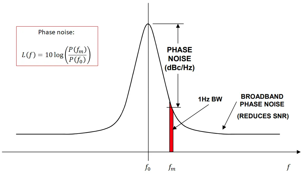
Phase noise describes the random phase fluctuations in a crystal oscillator's output signal, appearing as close-in and far-out sidebands around the carrier frequency in the frequency domain. Jitter, its time-domain counterpart, quantifies short-term variations in signal edges, directly impacting timing margins in high-speed circuits. These instabilities arise from inherent noise sources within the quartz resonator, amplification stages, and external perturbations like temperature changes or mechanical vibration. Frequency stability refers to the oscillator's ability to maintain nominal output over time, temperature, and supply variations, often quantified in parts per million. In high-speed circuits, excessive crystal oscillator phase noise degrades signal-to-noise ratios in receivers and increases bit error rates in serializers-deserializers. Addressing these metrics early in design prevents downstream issues in systems operating at multi-gigabit rates.
Low phase noise oscillators prioritize high-Q quartz crystals and optimized feedback networks to suppress flicker noise and thermal effects. TCXOs incorporate compensation circuits to counteract temperature-induced drifts, achieving stability suitable for portable high-speed devices. OCXOs use thermal ovens for even tighter control, ideal for base stations or precision instrumentation. Understanding the interplay between phase noise, jitter, and frequency stability guides selection and layout decisions. Engineers must balance these parameters against power, size, and cost constraints in dense PCB environments.
Key Factors Contributing to Phase Noise and Instability
Several mechanisms drive phase noise in crystal oscillators, starting with the resonator's intrinsic flicker noise, which dominates close-in performance. Power supply noise couples into the circuit, modulating the oscillation amplitude and frequency, while electromagnetic interference from nearby digital lines injects broadband noise. PCB parasitics, such as stray capacitance and inductance from long traces, alter the effective load and reduce negative resistance margin, leading to unstable startup or increased jitter. Temperature variations cause frequency pulling in uncompensated crystals, exacerbating phase noise through changes in quartz elasticity. Mechanical stress and vibration sensitivity further degrade performance by inducing microphonic effects.
In high-speed circuits, layout-induced coupling amplifies these issues, as high-frequency harmonics interact with oscillator traces. Supply ripple from switching regulators propagates through inadequate decoupling, directly worsening crystal oscillator phase noise. Ground bounce and return path impedance introduce common-mode noise, converting it to differential phase perturbations. Adhering to IPC-2221 guidelines for trace routing and layer stackup helps mitigate these by promoting controlled impedance and isolation. Quantifying these factors through simulation and measurement reveals priorities for intervention.
PCB Layout Best Practices for Low Phase Noise Oscillators
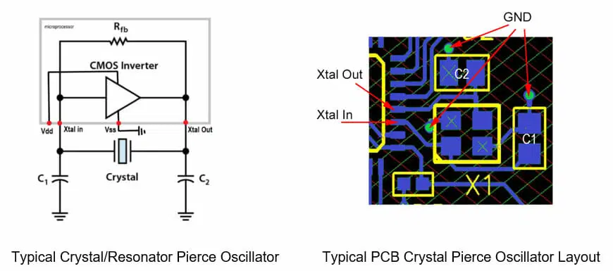
Optimal PCB layout begins with placing the crystal or oscillator module as close as possible to the driven IC pins, keeping interconnect traces under 10 mm to minimize parasitic inductance and capacitance. Symmetric routing for load capacitors ensures balanced loading, preventing mode hopping or frequency shifts. A continuous ground plane beneath the oscillator section provides low-impedance return paths, with multiple vias stitching it to deeper layers for effective noise shunting. Guard rings around the crystal and capacitors, connected via low-inductance vias, isolate the circuit from adjacent noise sources. Avoid routing high-speed signals or power lines under or near the oscillator to prevent capacitive coupling.
Decoupling capacitors, selected for low ESR, position directly at power pins with short, wide traces to ground, filtering high-frequency supply noise before it reaches the oscillator core. In multilayer boards, dedicate inner layers for ground and power planes, following IPC-7351 land pattern standards to ensure reliable soldering and minimal parasitics. For high-speed circuits, maintain trace widths for 50-ohm impedance where applicable, and use series resistors to tame edge rates without introducing excessive jitter. These practices collectively reduce crystal oscillator phase noise by preserving signal integrity from source to load.
Shielding via grounded metal cans over the oscillator further attenuates airborne EMI, especially in dense high-speed environments. Thermal vias under heat-generating components prevent localized heating that could pull frequency stability. Simulating the layout for parasitics refines these choices, confirming negative resistance exceeds five times the crystal's ESR for robust startup.
Component Selection and Power Supply Strategies
Selecting low phase noise oscillators involves matching drive level to the crystal's ratings, avoiding overdrive that accelerates aging and noise floor rise. TCXOs suit applications with moderate temperature swings, offering ppm-level stability without ovens, while OCXOs excel in precision needs despite higher power draw. Load capacitors must account for 2-5 pF PCB strays, using NP0 dielectrics for temperature insensitivity. Inverter gain stages provide sufficient transconductance for margin against process variations.
Power supply design emphasizes low-noise linear regulators over switchers near the oscillator, with multi-stage filtering using ferrite beads and capacitors spanning frequencies. Star grounding schemes separate analog and digital domains, uniting at a single point to prevent loops that amplify jitter. Voltage droop testing under load confirms stability, as supply modulation directly translates to phase noise.
Advanced Techniques: TCXO and OCXO Implementation
TCXOs integrate varactors and thermistors for active compensation, minimizing frequency stability errors across wide ranges. Their lower phase noise compared to basic XOs makes them viable for high-speed circuits like Ethernet PHYs. OCXOs maintain crystals at turnover temperature via heaters, achieving sub-ppb stability but requiring careful thermal isolation on PCBs. Hybrid approaches combine these with PLLs for multiplication while preserving close-in noise.
Layout for these modules mirrors basic oscillators but adds thermal management, such as copper pours for heat spreading without direct crystal contact. J-STD-001 assembly requirements ensure solder joints withstand vibration, preserving mechanical integrity. These implementations demand holistic design review for sustained low jitter.
Troubleshooting and Verification
Common issues include startup failure from insufficient drive or mismatched loads, resolved by measuring negative resistance margin. Elevated phase noise often traces to supply noise, verified by scoping ripple and adding filtering. Jitter in high-speed links points to EMI, addressed via shielding and rerouting. Environmental testing simulates real-world stresses, confirming frequency stability.
Conclusion
Maximizing crystal oscillator stability hinges on integrated design choices that suppress phase noise and jitter from the outset. PCB layout, component matching, and power strategies form the foundation, enhanced by TCXO or OCXO where demands exceed standard capabilities. Adopting these practices ensures reliable performance in high-speed circuits, reducing system-level errors and rework. Engineers achieve low phase noise oscillators through disciplined adherence to principles, yielding robust, future-proof designs.
FAQs
QX: What is crystal oscillator phase noise and why does it matter in high-speed circuits?
AX: Crystal oscillator phase noise refers to random phase fluctuations creating sidebands around the carrier, degrading spectral purity. In high-speed circuits, it increases jitter, lowers SNR, and raises BER in data links or ADCs. Minimizing it preserves timing margins and signal integrity. Proper PCB design and low-noise supplies are key mitigations. (52 words)
QX: How can PCB layout reduce jitter and improve frequency stability?
AX: Strategic placement near ICs, short symmetric traces, solid ground planes, and guard rings minimize parasitics and EMI coupling. Decoupling networks filter supply noise, while shielding blocks interference. These steps enhance negative resistance margin and load matching, stabilizing oscillation. Following IPC-2221 routing aids consistent results across prototypes. (58 words)
QX: What are the differences between TCXO and OCXO for low phase noise oscillators?
AX: TCXOs use electronic compensation for temperature drifts, offering ppm stability in compact, low-power packages suitable for high-speed portable devices. OCXOs employ ovens for ppb-level precision, ideal for fixed installations but with higher power and size. Both reduce phase noise over basic XOs, selected by environmental needs. (54 words)
QX: How to select components for optimal crystal oscillator phase noise performance?
AX: Choose crystals with low ESR and matching load capacitance, accounting for PCB strays. Prioritize high-Q cuts and stability specs like ±10 ppm. Pair with adequate inverter gain for margin. TCXOs or OCXOs extend capabilities for demanding frequency stability in high-speed circuits. Verify via simulation and measurement. (62 words)
References
IPC-2221B — Generic Standard on Printed Board Design. IPC, 2003
IPC-7351C — Generic Requirements for Surface Mount Design and Land Pattern Standard. IPC, 2010
J-STD-001H — Requirements for Soldered Electrical and Electronic Assemblies. IPC/JEDEC, 2018


