Introduction
Electromagnetic interference poses significant challenges in modern PCB designs, particularly as operating frequencies increase and component densities rise. Effective shielding component placement plays a crucial role in containing noise and protecting sensitive circuits. By strategically positioning shielding elements such as metal cans, ferrite filters, and guard traces, engineers can achieve optimal shielding design that enhances overall system reliability. This approach aligns with strategic PCB layout for EMI reduction, ensuring compliance with performance requirements while minimizing interference through component positioning. In this article, we delve into the principles and best practices tailored for electrical engineers designing high-performance boards. Understanding these techniques allows for proactive mitigation of EMI risks from the initial layout stage.
Understanding Shielding Component Placement and Its Importance
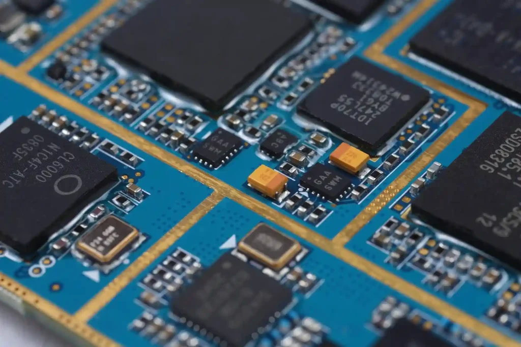
Shielding component placement refers to the deliberate arrangement of protective elements like conductive cans, decoupling capacitors, and ground vias relative to noise sources and sensitive signals on a PCB. These components form barriers that block or redirect electromagnetic fields, preventing unwanted coupling between circuits. Optimal shielding design integrates these elements seamlessly into the layout to confine emissions and susceptibility paths. In high-speed applications, poor placement can lead to radiated or conducted EMI that degrades signal integrity and fails regulatory tests.
The relevance of effective shielding placement techniques cannot be overstated in industries like telecommunications, automotive electronics, and medical devices. Strategic PCB layout for EMI reduction through component positioning directly impacts product performance, reducing debug time and rework costs during prototyping. For instance, grouping similar functions and isolating noisy sections minimizes crosstalk, while proper shield grounding ensures low-impedance paths for noise currents. As per IPC-2221 guidelines, maintaining adequate spacing between conductors supports these efforts by preventing unintended field interactions. Ultimately, mastering component placement for shielding elevates design quality and accelerates time-to-market.
Technical Principles Behind EMI and Shielding Effectiveness
Electromagnetic interference arises from three primary mechanisms: electric field coupling, magnetic field coupling, and radiated emissions. Electric fields couple capacitively between nearby traces or components, while magnetic fields induce currents through loops formed by return paths. Radiated EMI occurs when high-frequency currents on traces or planes act as antennas, propagating beyond the board. Component placement influences these by controlling proximity and loop areas, directly affecting field containment.
Shielding works by providing a low-impedance path that diverts currents away from sensitive areas, often leveraging Faraday cage principles at the board level. Ground planes adjacent to signal layers confine fields between them, reducing external radiation as per multilayer stackup best practices. Stitching vias around shielding perimeters create a continuous barrier, ensuring effective shielding placement techniques that block slot resonances. The effectiveness depends on material conductivity, enclosure completeness, and frequency; for example, openings must be small relative to the wavelength to avoid leakage.
Layer stackup plays a pivotal role, with signal layers sandwiched between ground or power planes offering superior isolation compared to microstrip routing. This configuration shields high-frequency signals from crosstalk, aligning with principles of minimizing interference through component positioning. Engineers must consider return path continuity, as discontinuities amplify emissions. These mechanisms underscore why initial placement decisions during schematic capture set the foundation for robust EMI performance.
Best Practices for Strategic PCB Layout and Shielding Integration
Begin with functional grouping during component placement for shielding, segregating digital, analog, and power sections to limit noise propagation. Place high-EMI sources like switching regulators and clock oscillators away from sensitive analog or RF circuits, ideally on opposite board sides if multilayer. This strategic separation reduces capacitive and inductive coupling, forming the basis of optimal shielding design. Maintain generous spacing per IPC-2221 standards for conductor clearance, especially around high-voltage or high-speed nodes.
Position decoupling capacitors as close as possible to IC power pins, minimizing inductive loops in the power delivery network. Use arrays of capacitors with varied values to cover broad frequency spectra, connecting directly to a solid ground plane via short vias. For effective EMI filtering, integrate LC or pi-filters at I/O ports and power entries, ensuring minimal trace lengths between filter and connector. These techniques exemplify minimizing interference through component positioning by suppressing noise at its origin.
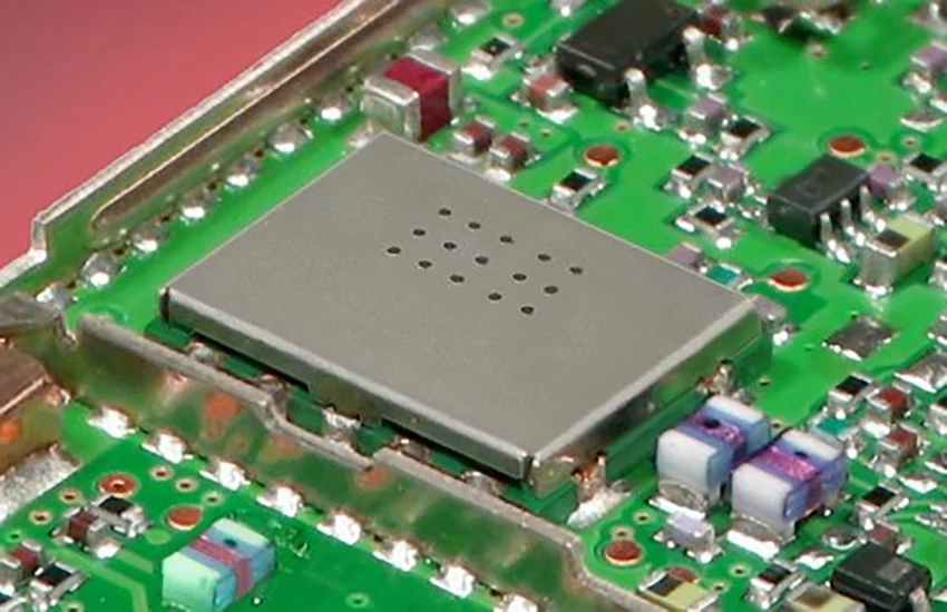
Implement board-level shielding cans over critical areas such as oscillators, RF receivers, or precision amplifiers. Secure cans with multiple low-impedance ground connections, surrounded by via fences spaced closely to form a perimeter shield. Provide adequate headroom around enclosed components to avoid assembly conflicts, incorporating the can footprint early in layout planning. Combine with copper pours tied to ground for enhanced field confinement, particularly along board edges.
Optimize layer stackup for shielding by placing ground planes adjacent to every signal layer, preferring six or more layers for complex designs. Employ stripline routing for noisy traces, embedding them between planes to tightly confine fields. Add stitching vias near signal transitions and board edges to maintain return path integrity and prevent edge radiation. Avoid split planes unless isolated sections connect at a single point, as splits can create high-impedance paths that radiate.
Guard traces and fences around sensitive signals further bolster strategic PCB layout for EMI reduction. Route guard traces parallel to signals, stitching them to reference planes with vias to absorb fringing fields. For mixed-signal boards, dedicate inner layers for analog grounds, bridging to digital grounds only at clean points. These practices ensure comprehensive coverage without overcomplicating the design.
Practical Insights: Troubleshooting Common Placement Pitfalls
Engineers often encounter EMI issues from overlooked placement details, such as clocks routed near board edges acting as antennas. Relocate generators centrally, shielded by cans and backed by ground planes underneath. Verify via stitching density around shields, as sparse placement allows field leakage. Simulate loop areas during review to identify and shrink them through rerouting.
In RF designs, align shielding cans precisely over modules, ensuring 360-degree grounding to chassis if applicable. Test for resonances by adjusting slot sizes in cans, keeping openings small. Component height mismatches under shields can cause shorts; use standoffs or custom profiles. These troubleshooting steps reinforce effective shielding placement techniques in real-world iterations.
Conclusion
Strategic component placement for shielding transforms PCB designs from vulnerable to resilient against EMI challenges. By prioritizing functional isolation, precise filter positioning, and integrated shielding cans with robust grounding, engineers achieve superior performance. Adhering to layered stackups and IPC-2221 spacing guidelines ensures manufacturability and reliability. Implementing these optimal shielding design principles minimizes debugging, enhances signal integrity, and supports high-speed operations. Electrical engineers equipped with these strategies can confidently tackle complex layouts, delivering boards that excel in demanding environments.
FAQs
Q1: What are the key considerations for component placement for shielding in high-speed PCBs?
A1: Group digital and power components separately from analog and RF sections to reduce coupling. Place decoupling capacitors directly adjacent to IC pins and shielding cans over noise sources like oscillators. Ensure ground planes underlie shielded areas with dense via stitching for low-impedance paths. This strategic PCB layout for EMI reduction confines fields effectively, improving overall EMC performance. Follow IPC-2221 for spacing to avoid unintended interactions.
Q2: How does optimal shielding design minimize interference through component positioning?
A2: Optimal shielding design involves positioning metal cans and ferrites close to emission sources while isolating sensitive circuits. Use guard traces and copper pours around critical signals, tied to adjacent ground planes. Minimize trace loops and edge proximity to prevent radiation. These effective shielding placement techniques, combined with multilayer stackups, block E and H fields, ensuring clean signals in dense boards.
Q3: Why is via stitching essential in strategic PCB layout for EMI reduction?
A3: Via stitching creates continuous ground return paths around shielding perimeters and signal transitions, confining high-frequency currents. Place stitches densely near layer changes and board edges to form fences that block slot resonances. This enhances shielding can effectiveness by providing multiple low-inductance connections. Proper implementation reduces radiated EMI significantly without adding layers.
Q4: What role does layer stackup play in effective shielding placement techniques?
A4: Layer stackup shields signals by sandwiching them between ground or power planes, limiting field spread. Position high-speed traces in striplines for tight confinement, avoiding microstrips on outer layers. Dedicate planes for analog and digital sections where possible. This foundation supports component placement for shielding, amplifying the benefits of cans and filters for comprehensive EMI control.
References
IPC-2221B — Generic Standard on Printed Board Design. IPC, 2003
IPC-6012E — Qualification and Performance Specification for Rigid Printed Boards. IPC, 2017


