Introduction
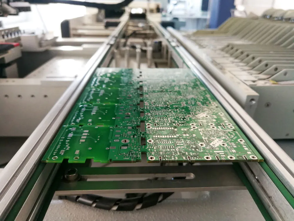
Surface mount technology (SMT) has revolutionized PCB assembly by enabling higher component densities and faster production rates. However, SMT yield issues remain a persistent challenge for electric engineers optimizing manufacturing lines. These problems often stem from defects introduced during key processes like solder paste printing, component placement, and reflow soldering. Addressing SMT assembly defects head-on can significantly boost first-pass yields, reduce rework costs, and ensure reliable electronic assemblies. In this article, we dive into the most common hurdles, their root causes, and proven troubleshooting strategies tailored for engineering teams. By focusing on practical interventions, engineers can transform potential failure points into strengths.
What Is SMT Assembly and Why Yield Matters
SMT assembly involves printing solder paste onto PCB pads, placing components precisely, and reflowing to form reliable joints. Yield in this context measures the percentage of boards passing inspection without defects after the full process. Low yields amplify production costs through scrap, rework, and delays, directly impacting project timelines for electric engineers. High yields, conversely, support scalable manufacturing and consistent performance in end applications. Engineers must prioritize yield optimization because even minor SMT assembly defects can cascade into field failures. Understanding these dynamics is crucial for designing robust processes from the outset.
Reflow soldering yield problems often dominate discussions, as this stage solidifies joints but exposes vulnerabilities like uneven heating. Industry benchmarks highlight that poor process control here accounts for a substantial portion of defects. Electric engineers benefit from viewing yield not just as a metric, but as a reflection of process maturity. Proactive yield management aligns with quality standards and enhances overall assembly efficiency.
Common SMT Assembly Defects
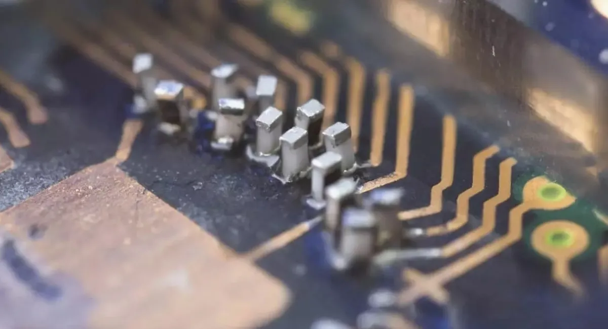
SMT assembly defects manifest in various forms, each tied to specific process weaknesses. Solder bridging occurs when excess paste connects adjacent pads, creating unintended shorts. This defect frequently arises during printing or reflow, compromising electrical isolation. Tombstoning, where one component end lifts during reflow, disrupts joint formation and signal integrity. Solder balls and beads scatter loose solder spheres, risking future shorts under vibration. These issues underscore surface mount technology (SMT) yield issues that demand vigilant inspection.
Insufficient solder or open joints result from inadequate paste volume or poor wetting, leading to weak mechanical and electrical connections. Component shift during placement or reflow misaligns parts, exacerbating non-wetting on pads. Voids trapped in solder joints reduce reliability by creating stress points. Warpage of the PCB or components distorts pad alignment, amplifying many of these defects. Electric engineers recognize these as interconnected challenges requiring holistic process tuning.
Root Causes of SMT Yield Issues
Surface mount technology (SMT) yield issues trace back to stencil printing inaccuracies, where poor aperture design leads to uneven paste deposition. Stencils with inadequate area ratios fail to release paste cleanly, causing bridging or insufficient volume at reflow. Component placement errors, such as offsets or rotations, compound when reflow dynamics shift parts. Reflow soldering yield problems often stem from improper thermal profiles, including ramp rates, soak times, and peak temperatures mismatched to component tolerances.
PCB warpage introduces mechanical stress, lifting pads during heating and promoting tombstoning or opens. Moisture sensitivity in components triggers popcorn effects, forming voids under rapid reflow heating. Solder paste rheology changes with storage or handling further degrade print quality. Electric engineers must analyze these causes systematically, as they interact across processes. Per IPC-A-610 guidelines, defect classification helps pinpoint origins without over-inspection.
Viscosity mismatches in paste or stencil wear contribute to beading and balls post-reflow. Thermal gradients across large boards exacerbate uneven melting, leading to cold joints. JEDEC J-STD-020E outlines moisture/reflow classifications to mitigate sensitivity-related failures. Tracing defects to these mechanisms enables targeted corrections.
Best Practices for Maximizing SMT Yield
Optimize SMT stencil design first, targeting area ratios around 0.6 to 0.7 for reliable paste release. Use laser-cut or electroformed stencils with appropriate thickness for fine-pitch components to minimize bridging risks. Validate prints with solder paste inspection (SPI) to catch volume anomalies early. For placement, calibrate machines for sub-50-micron accuracy and verify fiducials to prevent shifts.
Refine reflow profiles to match component classifications, ensuring gradual preheat to evaporate fluxes without splatter. Profile ovens regularly to maintain zone temperatures within 5 degrees Celsius variation. Implement nitrogen atmospheres to reduce oxidation and improve wetting. IPC J-STD-001 requirements guide soldering criteria for consistent joints. Post-reflow, automated optical inspection (AOI) flags defects before downstream issues.
Control incoming materials rigorously: store paste under refrigeration and components in dry cabinets per MSL ratings. Bake boards pre-assembly to eliminate absorbed moisture. Fixture warped panels during printing and reflow to maintain planarity. Layered inspections, from SPI to X-ray for voids, build yield confidence. Electric engineers should iterate process windows using design of experiments for peak performance.
Troubleshooting SMT Assembly Defects
When SMT assembly defects spike, start with defect mapping to correlate failures by location or lot. Bridging clusters near fine-pitch areas signal stencil cleaning or pressure adjustments. Tombstoning hotspots indicate pad imbalance or rapid reflow ramps; symmetrize designs and slow heating. Voids persisting post-nitrogen suggest flux activation issues or MSL violations.
For reflow soldering yield problems, thermocouple boards to validate profiles against simulations. Warpage exceeding 0.75% triggers lamination reviews or thinner cores. Shifted components prompt feeder checks and vision system tweaks. Document root causes in a Pareto chart for recurring patterns. Cross-reference with IPC-A-610 criteria to classify and prioritize.
Real-world troubleshooting reveals that 70% of yield gains come from print and reflow tweaks. To maximize efficiency, these findings must be integrated into high-performance PCB assembly key design considerations early in the project lifecycle. Simulate defects in software to predict sensitivities pre-production, and collaborate across design, process, and quality for closed-loop improvements that define the next generation of hardware.
Conclusion
Tackling surface mount technology (SMT) yield issues demands a multifaceted approach centered on defect prevention and process control. By addressing SMT assembly defects through precise stencil work, optimized reflow, and rigorous inspections, engineers achieve yields above 99%. Reflow soldering yield problems diminish with profile mastery and material handling discipline. Standards like IPC-A-610, JEDEC J-STD-020E, and IPC J-STD-001 provide the framework for excellence. Electric engineers equipped with these strategies deliver robust assemblies ready for demanding applications. Prioritize yield as a core metric to drive manufacturing success.
FAQs
Q1: What are the most common surface mount technology (SMT) yield issues?
A1: SMT yield issues primarily include solder bridging, tombstoning, insufficient joints, and voids. These arise from printing inaccuracies, placement errors, and reflow profile mismatches. Troubleshooting starts with SPI and AOI to isolate causes. Optimizing stencil apertures and thermal ramps resolves most cases efficiently. Yield improves through iterative process validation.
Q2: How do SMT assembly defects impact PCB reliability?
A2: SMT assembly defects like opens or bridges create intermittent failures under thermal cycling or vibration. Voids weaken joints mechanically, accelerating fatigue. Early detection via IPC-A-610 inspections prevents field escapes. Engineers mitigate by refining paste volume and reflow conditions for uniform wetting.
Q3: What causes reflow soldering yield problems in SMT?
A3: Reflow soldering yield problems stem from improper preheat, peak temperatures exceeding component limits, or moisture in parts. Warpage and flux burnout lead to non-wetting or balls. Follow JEDEC J-STD-020E for MSL handling and profile to classification. Nitrogen use and oven zoning enhance consistency.
Q4: How can electric engineers maximize SMT yields?
A4: Electric engineers maximize SMT yields by standardizing stencil designs, validating reflow profiles, and layering inspections. Address root causes like warpage with fixtures and baking. IPC J-STD-001 guides soldering practices. Continuous monitoring and DOE yield sustained gains above 98%.
References
IPC-A-610H — Acceptability of Electronic Assemblies. IPC, 2019
JEDEC J-STD-020E — Moisture/Reflow Sensitivity Classification for Nonhermetic Solid State Surface Mount Devices. JEDEC, 2014
IPC J-STD-001H — Requirements for Soldered Electrical and Electronic Assemblies. IPC, 2018


