Introduction
High-frequency PCBs operate in environments where signals reach GHz ranges, making electromagnetic interference (EMI) a critical concern for reliable performance. Shielding components play a vital role in containing radiated emissions and preventing susceptibility from external fields, especially in RF circuits and high-speed designs. Selecting the right high-frequency PCB shielding components ensures compliance with electromagnetic compatibility requirements while maintaining signal integrity. Poor shielding choices can lead to crosstalk, noise coupling, and failure in applications like wireless communication and radar systems. This guide explores the principles, materials, and techniques for effective EMI reduction in GHz PCBs. Engineers can apply these structured insights to optimize designs for demanding frequencies.
Understanding EMI in High-Frequency PCBs
Electromagnetic interference arises from unintended coupling between circuits or external sources, manifesting as conducted noise through power lines or radiated emissions via antennas formed by traces. In high-frequency applications, shorter wavelengths exacerbate issues, as even small discontinuities act as efficient radiators. GHz signals experience significant attenuation losses and reflections without proper mitigation, leading to bit errors in digital links or degraded modulation in analog RF paths. Shielding components block these fields by providing a conductive barrier that redirects or absorbs energy. Understanding the distinction between electric and magnetic field dominance at different frequencies guides component selection. For instance, electric fields prevail above 100 MHz, favoring high-conductivity enclosures.
Principles of Shielding Effectiveness
Shielding effectiveness (SE) quantifies attenuation in decibels, comprising reflection loss from impedance mismatch, absorption loss within the material thickness, and multiple reflection corrections for thin shields. The skin depth, defined as the distance where field amplitude drops to 1/e, decreases with frequency, conductivity, and permeability, dictating minimum shield thickness. At GHz frequencies, absorption dominates for good conductors, while magnetic materials enhance low-frequency performance. Engineers calculate SE using SE = 20 log (reflection + absorption factors) to predict performance. Proper design minimizes apertures and seams, as leakage scales with wavelength. Adhering to IPC-2221 guidelines for trace routing and plane placement supports these principles in PCB layouts.
Types of Shielding Components for High-Frequency PCBs
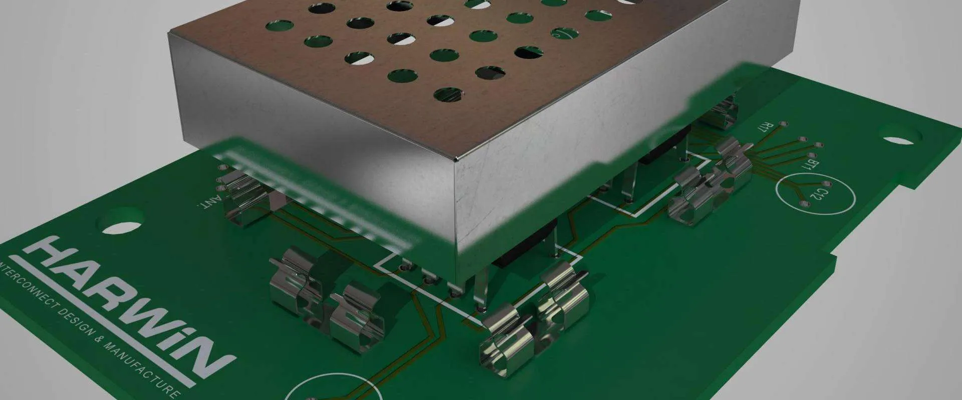
Common shielding components include metal cans or lids that enclose sensitive areas, providing full cavity protection against broad-spectrum EMI. Fence structures, formed by perimeter walls or stamped metal frames, offer compartmentalization for multiple modules on a single board. Conductive gaskets or elastomers seal interfaces between shields and boards, compensating for tolerances in assembly. Vias arranged in fencing patterns around traces create distributed barriers, ideal for embedded shielding without added height. Each type suits specific needs, such as cans for maximum isolation or vias for cost-sensitive designs. Selection depends on space constraints and frequency, with cans excelling in GHz PCBs due to seamless coverage.
Key Criteria for Selecting Shielding for RF Circuits
Frequency range dictates material and thickness, as higher GHz demands thinner skins but robust seams smaller than lambda/20. Required SE targets, often 40-60 dB for commercial RF, balance against size, weight, and thermal dissipation. Mechanical robustness ensures survivability during vibration or thermal cycling, while solderability affects assembly yield. Corrosion resistance influences longevity in humid environments, favoring tin-plated options. Cost-effectiveness weighs volume production against performance gains. Engineers prioritize low-inductance grounding paths to multiple board points, avoiding single-point connections that create loops.
Best Shielding Materials for High-Speed Designs
Copper offers superior conductivity for reflection-dominant shielding at high frequencies, forming the basis for foils and cans in most RF applications. Nickel plating adds magnetic permeability and corrosion protection, enhancing absorption for mixed spectra. Tin coatings improve solder wetting without compromising SE, common on formed shields. Aluminum suits lightweight needs with adequate performance up to several GHz, though oxidation requires anodizing. Conductive polymers or paints enable conformal coatings on irregular surfaces, flexible for prototypes. Material choice aligns with skin depth requirements, ensuring thickness exceeds 3-5 times delta for optimal absorption.
Advanced PCB Shielding Techniques for EMI Reduction in GHz PCBs
Via shielding involves stitching ground vias along signal perimeters at spacings below lambda/10, effectively creating a Faraday cage in multilayer stacks. Cavity resonance control uses internal partitions or absorbers to suppress modal peaks in enclosed volumes. Honeycomb vents permit airflow while attenuating waves above cutoff frequencies proportional to cell size. Embedded metal planes between layers provide baseline isolation, augmented by moat cuts to segment grounds. These techniques integrate seamlessly in high-density interconnects, minimizing profile. IEC 61000 series testing validates radiated immunity post-implementation.
Practical Implementation and Best Practices
Position shields over noise sources like clock generators or power amplifiers first, extending coverage to victim circuits. Multiple ground vias, spaced at lambda/4 or closer, shunt currents effectively without inductance buildup. Avoid slots or perforations larger than lambda/20 perpendicular to fields. Thermal vias under shields dissipate heat from enclosed ICs, preventing hotspots. Post-assembly verification uses near-field probes to map leakage before full chamber tests. Layer stackups with dedicated ground planes adjacent to signals form the foundation, per IPC-2221 recommendations.
Common Challenges and Troubleshooting
Seam gaps from warpage or tolerance stackup leak energy, addressed by compressible gaskets or adjustable clips. Ground bounce couples through shared returns, mitigated by partitioned planes tied at single low-impedance points. Over-shielding traps heat, requiring vents or cutouts with mesh. Multipaction in vacuum applications erodes surfaces at GHz, demanding smooth finishes. Troubleshooting starts with spectrum analysis to isolate frequencies, then targeted modifications. Iterative simulation refines before fabrication.
Conclusion
Selecting high-frequency PCB shielding components demands a systematic approach balancing SE, materials, and integration. From cans and fences to via arrays and advanced cavities, each technique contributes to robust EMI reduction in GHz PCBs. Prioritizing principles like skin depth and aperture control ensures high-speed designs meet performance goals. Engineers benefit from standards-guided practices for repeatable success. Implementing these strategies enhances reliability in RF circuits, paving the way for next-generation electronics.
FAQs
Q1: What are the primary high-frequency PCB shielding components for RF circuits?
A1: High-frequency PCB shielding components include metal cans, fences, gaskets, and via fences. These enclose sensitive areas to block radiated EMI. Selection hinges on frequency, with cans providing broad isolation and vias suiting multilayer boards. Proper grounding maximizes effectiveness, ensuring low-impedance paths. This approach aligns with design standards for GHz operation.
Q2: How do you achieve EMI reduction in GHz PCBs using shielding?
A2: EMI reduction in GHz PCBs relies on materials with adequate skin depth and seamless enclosures. Reflection and absorption losses attenuate fields effectively. Minimize apertures and use multiple ground connections. Advanced techniques like cavity partitioning suppress resonances. Testing confirms compliance without over-design.
Q3: What are the best shielding materials for high-speed designs?
A3: Best shielding materials for high-speed designs feature high conductivity like copper for GHz reflection loss. Nickel enhances magnetic absorption, tin aids assembly. Thickness exceeds skin depth for optimal SE. Aluminum offers weight savings with trade-offs in corrosion. Match to application spectra for efficiency.
Q4: What advanced PCB shielding techniques improve performance?
A4: Advanced PCB shielding techniques include via stitching, honeycomb vents, and embedded planes. These create distributed barriers reducing crosstalk. Control cavity modes with absorbers or partitions. Integrate early in stackup planning. Such methods excel in dense RF layouts for superior isolation.
References
IPC-2221 — Generic Standard on Printed Board Design. IPC
IEC 61000-4-3 — Electromagnetic compatibility (EMC) - Part 4-3: Testing and measurement techniques - Radiated, radio-frequency, electromagnetic field immunity test. IEC
IPC-6012E — Qualification and Performance Specification for Rigid Printed Boards. IPC, 2017


