Introduction
In modern electronics, high-speed circuits demand precise control over signal propagation and electromagnetic interference to achieve reliable performance. An 8-layer PCB stack-up provides the necessary complexity to support dense routing, multiple reference planes, and dedicated power distribution layers. This configuration excels in applications like telecommunications, computing, and data processing where frequencies exceed several gigahertz. Engineers must prioritize signal integrity and EMI reduction during the design phase to prevent issues such as crosstalk, reflections, and radiation. By optimizing the PCB stack up, designers can balance electrical performance with manufacturability constraints. This article explores advanced techniques for 8-layer PCB design tailored to high-speed requirements.
What Is an 8-Layer PCB Stack-Up and Why It Matters for High-Speed PCBs
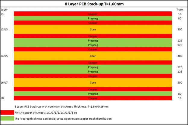
An 8-layer PCB stack-up consists of eight conductive copper layers separated by insulating cores and prepregs, forming a symmetric or asymmetric arrangement to meet specific electrical needs. Each layer serves a distinct purpose, such as signal routing, ground referencing, or power delivery, with the overall thickness typically ranging from 1.6 mm to 2.4 mm depending on application demands. In high-speed PCB contexts, this multilayer structure allows for stripline and microstrip transmission lines that maintain controlled impedance over long traces. The added layers compared to 4- or 6-layer boards enable better isolation between sensitive signals and noisy power sections. Consequently, 8-layer designs reduce loop areas for return currents, minimizing EMI emissions that could violate regulatory limits. For electric engineers, mastering 8-layer PCB design ensures compliance with performance specs in demanding environments.
The relevance stems from the exponential growth in data rates, where even minor stack-up flaws lead to bit errors or system failures. Proper plane pairing provides low-inductance paths essential for gigabit signals. Without adequate planes, high-speed signals suffer from increased insertion loss and jitter. Thus, the stack-up directly influences the board's ability to handle rise times below 100 ps.
Key Technical Principles in 8-Layer PCB Stack-Ups for High-Speed Performance
The foundation of high-speed PCB stack-ups lies in providing continuous reference planes adjacent to signal layers to confine electromagnetic fields. In stripline configurations, signals embedded between two planes experience uniform dielectric surroundings, promoting consistent characteristic impedance around 50 ohms single-ended or 100 ohms differential. Microstrip lines on outer layers couple primarily to a single plane, requiring thinner dielectrics for impedance control. Core and prepreg materials must exhibit low dissipation factors to limit signal attenuation at frequencies above 1 GHz. Symmetry in the stack-up prevents warpage during fabrication and assembly, as unbalanced copper distribution induces mechanical stress.
Return path integrity forms another critical principle, where ground planes capture the majority of return currents to avoid broadside coupling between parallel traces. Via transitions demand blind or buried vias to preserve reference continuity across layers. Plane capacitance between power and ground pairs acts as a distributed decoupling network, stabilizing voltage rails under transient loads. These mechanisms collectively enhance signal integrity by reducing reflections from impedance discontinuities.
Common 8-Layer Stack-Up Configurations for High-Speed Circuits
A prevalent configuration pairs outer signal layers with inner ground planes for microstrip routing, followed by internal signal layers in stripline. For instance, layer 1 (top signal), layer 2 (ground), layer 3 (signal), layer 4 (power), layer 5 (power), layer 6 (signal), layer 7 (ground), and layer 8 (bottom signal) offers balanced power distribution. This setup dedicates two ground planes for shielding high-speed signals while splitting power into separate planes to isolate analog and digital domains. Prepreg thicknesses between signal and plane layers control impedance, typically thinner for outer layers to compensate for air dielectric effects.
Another variant emphasizes more ground planes, such as layer 2 and layer 7 as primary grounds, with layer 4 and layer 6 as power planes adjacent to signals. This arrangement minimizes crosstalk by increasing plane-signal-plane separation for slower nets while tightening it for critical high-speed pairs. Engineers adjust core thicknesses to achieve overall board rigidity and thermal expansion matching. Such configurations align with IPC-2221 guidelines for multilayer board design, ensuring viable fabrication yields.
In high-density interconnect scenarios, hybrid stack-ups incorporate thinner inner layers for fine-pitch routing, reserving thicker cores for structural integrity. Selection depends on pin count, data rates, and power requirements, always prioritizing adjacent plane referencing.
Advanced Techniques for Signal Integrity in 8-Layer PCB Design
To optimize signal integrity, length matching within 0.5% applies to differential pairs across layers, compensating for via stubs through back-drilling. Orthogonal routing between adjacent signal layers reduces broadside crosstalk, while guard traces on the same layer shield sensitive nets. Reference plane partitioning with moats and stitching vias prevents slots that disrupt return paths, especially near connectors. Simulation verifies eye opening margins before layout finalization.
For multi-gigabit interfaces, embedded transmission lines in stripline layers outperform microstrips due to lower radiation losses. Controlled dielectric constant uniformity across prepregs ensures predictable propagation delays. Vias optimized with taper transitions minimize inductance, preserving rise times.
Strategies for EMI Reduction in High-Speed 8-Layer PCB Stack-Ups
EMI reduction relies on dedicating full ground planes to capture displacement currents, forming a Faraday cage-like enclosure around signals. Power plane splits must include overlap regions coupled by capacitors to avoid radiating edges. Stitching vias along partition boundaries bridge ground planes, shunting high-frequency currents effectively. Minimizing trace lengths on outer layers curtails loop antenna effects.
Interplane capacitance between adjacent power-ground pairs provides broadband filtering, reducing simultaneous switching noise. Segregating clocks and high-edge-rate signals to inner layers shields them from external coupling. Compliance with IPC-6012 performance specifications guides layer thickness tolerances to maintain shielding effectiveness. These techniques lower radiated emissions without excessive shielding materials.
Best Practices for Implementing 8-Layer PCB Stack-Ups
Start with symmetric constructions to equalize copper on both sides, mitigating bow and twist per industry norms. Select low-loss dielectrics with dielectric constants around 3.5 to 4.5 for high-speed layers, ensuring via aspect ratios below 10:1 for reliable plating. Define trace widths and spacings early based on stack-up calculations for target impedances. Incorporate split planes judiciously, with at least 20% overlap for current sharing.
Fabrication drawings specify sequential lamination to control inner layer registration. Post-design reviews focus on plane voids near high-current paths to prevent hotspots. Prototype testing validates stack-up assumptions through TDR measurements and near-field scans. Adhering to J-STD-001 criteria during assembly preserves integrity.
Common Challenges and Troubleshooting in 8-Layer High-Speed Designs
Warpage emerges from asymmetric CTE mismatches between cores and prepregs, addressed by balancing layer pairings. Signal skew across layers requires serpentine tuning constrained by routing channels. Power delivery noise propagates through thin dielectrics, necessitating dense decoupling arrays. Troubleshooting involves S-parameter analysis to isolate resonances.
Fabrication tolerances on prepreg flow can alter impedances by 10%, demanding statistical modeling. Thermal vias under ICs manage heat spreading across planes without compromising references.
Conclusion
An optimized 8-layer PCB stack-up unlocks superior performance for high-speed circuits by integrating robust signal integrity and EMI reduction measures. Strategic layer assignment, plane referencing, and symmetry form the core of effective designs. Engineers benefit from following established principles to navigate complexity while ensuring manufacturability. Implementing these techniques elevates board reliability in next-generation systems. Prioritize simulation and validation to refine stack-ups iteratively.
FAQs
Q1: What is a typical 8-layer PCB stack up for high-speed applications?
A1: A common 8-layer PCB stack up features signal layers on the top and bottom adjacent to ground planes, with inner signals sandwiched between power and ground for stripline routing. This configuration provides dedicated reference planes for impedance control and EMI shielding. Power planes occupy central layers to distribute current evenly. Such arrangements support data rates beyond 10 Gbps while maintaining signal integrity through low-loss paths.
Q2: Why choose an 8-layer PCB design over fewer layers for high-speed PCBs?
A2: 8-layer PCB designs offer additional ground and power planes, enabling better isolation for differential pairs and reduced crosstalk compared to 6-layer boards. They accommodate denser routing without compromising return path integrity. EMI reduction improves due to enclosed fields in striplines. Overall board thickness supports mechanical stability under thermal cycling.
Q3: How does PCB stack up impact signal integrity in high-speed circuits?
A3: PCB stack up determines impedance consistency and field confinement, directly affecting reflections and jitter in high-speed signals. Adjacent planes minimize loop inductance for clean return currents. Uniform dielectrics prevent delay skew. Poor stack-ups amplify crosstalk, degrading eye diagrams.
Q4: What are key strategies for EMI reduction in 8-layer PCB design?
A4: Key strategies include full ground planes next to signals, stitching vias at splits, and orthogonal inner layer routing to suppress coupling. Power-ground capacitance filters noise effectively. Minimizing outer layer traces reduces radiation. These ensure compliance with emission standards.
References
IPC-2221B — Generic Standard on Printed Board Design. IPC, 2009
IPC-6012E — Qualification and Performance Specification for Rigid Printed Boards. IPC, 2017
IPC-A-600K — Acceptability of Printed Boards. IPC, 2020
J-STD-001G — Requirements for Soldered Electrical and Electronic Assemblies. IPC, 2017