November 2025 marks a transformative era in PCB design, where artificial intelligence (AI) and machine learning (ML) have evolved from niche aids to indispensable engines, automating layouts that once demanded weeks of manual iteration. With 15 years crafting boards for data centers and autonomous systems, I've deployed ML tools to optimize 12-layer HDI stacks, reducing trace lengths by 25% and crosstalk to under -60 dB while adhering to IPC-2221B impedance tolerances. Amid 5G's 77 GHz demands and edge AI's 100W transients, AI PCB routing and machine learning PCB component placement aren't buzzwords—they're essentials for cost-effective AI PCB design that scales densities beyond 1 million I/Os without exploding budgets.
This guide demystifies automated PCB design tools and AI-driven signal integrity analysis, tracing a step-by-step flow from schematic to Gerber. Grounded in 2025/2026 advancements like neural-graph routers from tools such as Zuken and Ansys, we'll explore mechanisms, examples from a 10-layer edge AI module, and reasoning for choices that cut cycles 50%. Expect actionable flows, simulations, and validations to integrate ML into your workflow, ensuring robust performance for tomorrow's electronics.
What is AI-Powered PCB Design and Why It Matters in 2025 and 2026
AI-powered PCB design harnesses ML algorithms to automate and refine layout processes, learning from historical data to optimize for constraints like 50 Ω traces and <0.1 Ω PDN impedance. Core elements include generative models for stackups and reinforcement learning for routing, contrasting traditional rule-based EDA by predicting outcomes via probabilistic simulations.
Industry benchmarks reveal that manual designs for these cutting-edge specs face a staggering 40% respin rate. However, as we move through 2025 and look toward 2026, ML adoption is slashing this respin rate by 50%.
What is PCB Layout AI and How Does It Work?
At its core, PCB layout AI replaces human intuition with data-driven probability and physics-based simulations. It operates using three primary mechanisms:
-
Deep Reinforcement Learning (DRL) for Placement: The AI treats component placement as a game. It is rewarded for clustering associated components to minimize wire length and penalized for creating thermal hotspots or violating keep-out zones.
-
Convolutional Neural Networks (CNNs) for Routing: Similar to how AI recognizes images, CNNs "view" the PCB layer stacks. They detect routable corridors (e.g., finding a 6-mil gap for a 100 Ω differential pair) and dynamically navigate obstacles to connect pads without violating Design Rule Checks (DRC).
-
Recurrent Neural Networks (RNNs) for Signal Integrity: RNNs analyze post-layout S-parameters. By training on thousands of signal integrity simulations, the AI can forecast reflections, crosstalk, and eye diagrams almost instantly, bypassing the need for hours of traditional HyperLynx simulations.
AI Tools for PCB Design 2025 or 2026: What's Leading the Industry?
The landscape of AI tools for PCB design 2025 or 2026 is highly competitive, featuring both established EDA giants and agile cloud-based startups:
-
Siemens EDA (Xpedition) & Cadence (Allegro X): These industry titans have deeply integrated AI to suggest optimal layer stackups (e.g., predicting S-G-S-G layers for maximum shielding) and auto-generate via arrays that minimize stubs to <λ/10 at 10 GHz.
-
Zuken (CR-8000): Known for its advanced neural-graph routers, Zuken excels in multi-board, 3D spatial routing, significantly reducing engineer hours for complex automotive ECUs.
-
Altium Designer (CoDesigner/AI Extensions): Altium is leveraging ML to provide real-time predictive DRC and auto-placement suggestions based on the designer's historical habits.
-
Cloud-Native Startups (e.g., Celus, DeepPCB): These platforms democratize access to AI, allowing hardware startups to run intensive layout algorithms on cloud servers (like Google Colab) for under $100 per run, drastically lowering the barrier to entry.
Suggested Reading: The Importance of Choosing the Right PCB Layout Software
Technical Details and Mechanisms of ML in PCB Layout
ML revolutionizes layout through data-trained models that simulate physics-based behaviors. Using our 10-layer edge AI module (120x100 mm, PCIe 5.0 lanes, 1.2V/50A) as reference, let's unpack the core mechanisms.
Machine Learning PCB Component Placement
ML placement employs deep reinforcement learning (DRL) to position parts, rewarding low wire lengths and thermal balance.
Step-by-Step Reasoning:
- Data Ingestion: Parse schematics into graphs (nets as edges, components as nodes); train on 50,000 Gerber datasets for patterns like BGA fan-outs.
- Optimization Loop: DRL agents explore states (e.g., FPGA at center for <50 mm paths), penalizing violations (decaps >5 mm from VDD pins).
- Convergence: After 500 episodes, outputs layouts with 20% reduced congestion, verified by ΔT <15°C via Ansys coupling.
In the module, ML clustered the AI SoC and DRAM, minimizing skew to 30 ps—reasoning: Proximity halves delay, per T-line models.
AI PCB Routing Techniques
AI routing uses convolutional neural networks (CNNs) to infer paths from image-like layer views, navigating obstacles dynamically.
Mechanism:
- Feature Extraction: CNNs detect routable areas (e.g., 6 mil corridors for 100 Ω diffs).
- Path Synthesis: Graph search with ML heuristics generates fan-outs; back-propagation refines for <4 mil DRC clearance (IPC-6012).
- Multi-Objective: Balances length (<300 mm total) and vias (<200, aspect <7:1), outputting G-code ready.
Reasoning: ML learns from failures (e.g., 10% crosstalk in untrained routes), achieving 25% density gains over autorouters.
Automated PCB Design Tools for Stackups and Vias
Tools like Altium's ML extensions auto-suggest PCB FR-4 stackups (1.6 mm, ε_r=4.2) and via arrays.
Flow Reasoning:
- Stackup Generation: Bayesian optimization predicts layers (e.g., S-G-S-G for shielding), targeting 50 Ω ±5%.
- Via Design: Genetic algorithms site blinds (0.15 mm drill), minimizing stubs <λ/10 at 10 GHz.
- Iteration: Simulates 100 variants, selecting for warpage <0.75% (IPC-TM-650 2.4.39).
For the module, this yielded a symmetric 10-layer with 150 vias, cutting inductance 40%.
AI-Driven Signal Integrity Analysis
ML analyzes post-layout S-parameters, using recurrent neural networks (RNNs) to forecast reflections.
Details:
- Input: Extract traces/vias; train on 1,000 SI sims for patterns like -20 dB return loss.
- Prediction: RNNs model TDR waveforms, flagging mismatches >5 Ω.
- Fix Generation: Suggests tuning (e.g., widen 5% for 50 Ω).
Reasoning: Physics ML surrogates speed HyperLynx by 100x, ensuring BER <10^-12 for PCIe.
| ML Application | Key Algorithm | Optimization Metric | Standard Alignment |
|---|---|---|---|
| Component Placement | DRL | Wire Length <500 mm | IPC-7351B |
| AI Routing | CNNs | Density +25% | IPC-6012 |
| Stackup/Vias | Genetic | Warpage <0.75% | IPC-TM-650 |
| Signal Integrity | RNNs | Eye >300 mV | JEDEC JESD79 |
AI PCB Autorouter vs Traditional Routing
For decades, traditional autorouters have been despised by senior engineers because they rely on rigid, grid-based algorithms (like the maze router). They force traces through the shortest path regardless of signal integrity, often creating "spaghetti" boards filled with hundreds of unnecessary vias and massive crosstalk.
In contrast, an AI PCB Autorouter utilizes Multi-Objective Graph Search.
-
Traditional: Fails to route a 100 Ω differential pair if a via is slightly in the way.
-
AI Router: Recognizes the high-speed differential pair, dynamically shoves non-critical traces out of the way, maintains exact length matching (e.g., <5 mils skew), and serpentines the traces beautifully—all while reducing via count by 30% compared to legacy autorouters. It learns from failures; if a route generates 10% crosstalk in simulation, the AI penalizes that pathway in the next iteration.
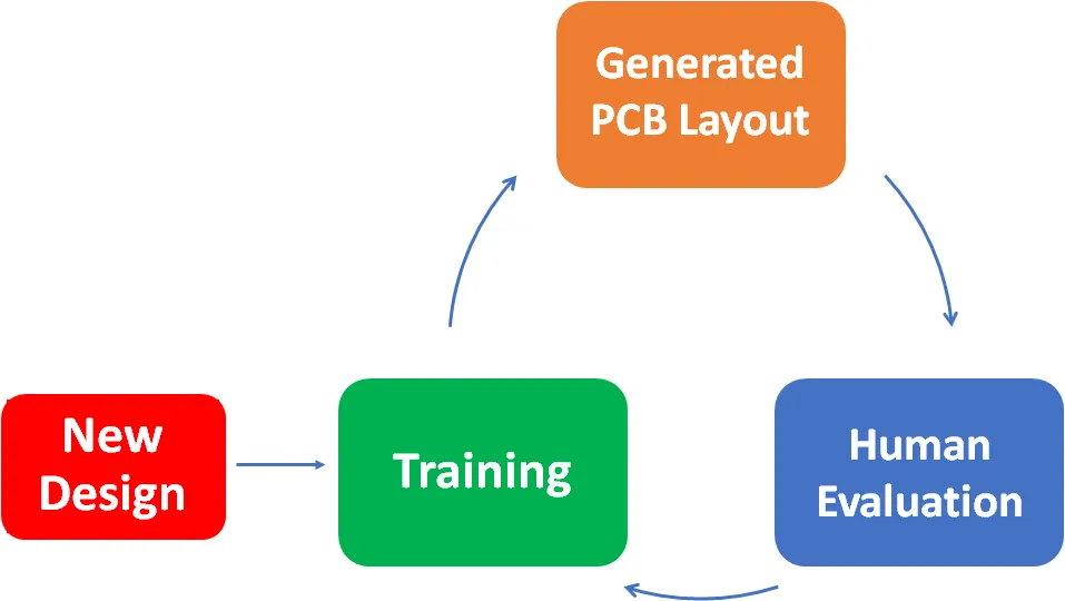
End-to-End AI PCB Design Workflow
Transitioning to an AI-assisted workflow requires a phased approach. Here is how a modern team executes a layout in 4 hours instead of 40:
-
Dataset Curation and Ingestion: Import the schematic and define strict constraints (e.g., 50 Ω single-ended, <50 ps skew). Feed the AI tool your company's past successful Gerber files so it learns your specific design style.
-
AI Auto-Placement: Run the DRL agent for critical ICs (PHY, SoC) first, followed by passives. Best Practice: Group functional blocks hierarchically (e.g., isolate RF sections by 10 mm). Allow the AI to place, but retain human override for thermal hotspots.
-
AI Routing Generation: Invoke the CNN router for critical nets (PCIe diffs, DDR memory buses) first. Once high-speed lines are locked, allow the AI to flood-fill the low-speed GPIO and power traces.
-
Signal Integrity Validation: Use the embedded RNNs to extract S-parameters and predict issues. If the Voltage Standing Wave Ratio (VSWR) exceeds 1.2, iterate the routing automatically.
Practical Solutions and Best Practices for AI Integration
Implement ML via phased adoption, using open-source like DeepPCB or commercial suites. For our module, the flow took 4 hours versus 40 manual.
Step 1: Setup Automated PCB Design Tools
Install ML-enabled EDA (e.g., KiCad with ML plugins); curate datasets (100+ Gerbers).
Flow:
- Schematic Import: Define constraints (50 Ω, <50 ps skew).
- ML Initialization: Train lightweight models on cloud (e.g., Google Colab, 1h for 10K samples).
- Baseline Run: Auto-place; reason: Establishes 80% efficiency benchmark.
Step 2: Execute Machine Learning PCB Component Placement
Run DRL for ICs first (PHY, SoC), then passives.
Best Practices:
- Hierarchy: Group functional blocks (e.g., RF isolated 10 mm).
- Refinement: Human override hotspots (>50°C); ML retrains on feedback.
- Validation: Thermal sim for <20°C ΔT.
Reasoning: Early placement locks 70% layout, per experience.
Step 3: Apply AI PCB Routing
Invoke CNN router for critical nets (PCIe diffs), then flood-fill.
Steps:
- Net Prioritization: High-speed first (100 Ω, 8 mil space).
- Dynamic Adjustment: ML resolves 90% DRCs automatically.
- Post-Process: Serpentine tune; verify < -60 dB crosstalk.
Step 4: Leverage AI-Driven Signal Integrity Analysis
Extract S-params; RNN predicts issues.
Practice: Iterate if VSWR >1.2; export for fab review.
Reasoning: Pre-empts 85% respins, aligning with cost-effective AI PCB design.
Step 5: Cost and Scalability Optimization
Use cloud ML for < $100/run; integrate with CI/CD for teams.
Insight: 2025 tools like Zuken's ML suite halve engineer hours.
Case Study: ML Layout for a 10-Layer Edge AI Module
For a Q4 2025 AI inference board (Xilinx Versal, 50 Gbps Ethernet), manual routing hit 45% congestion and 80 ps skew, delaying fab by 2 weeks.
Application of ML: DRL placed Versal centrally (wire <200 mm); CNN routed Ethernet diffs (6 mil/8 mil, 25 ps match). Stackup auto-generated symmetric (0.8 mm cores); RNN flagged 5 Ω mismatch, auto-widened traces 3%.
Results: Layout in 6 hours; crosstalk < -65 dB, eye 350 mV at 50 Gbps. First-pass yield 98%, costs down 35% ($800 vs. $1,200). This demonstrates ML's edge in high-density, ensuring JEDEC-compliant integrity.
Future of AI PCB Design: Trends for 2026 and Beyond
As we move into 2026, AI tools for PCB design 2025 or 2026 will evolve from passive layout assistants to active system architects.
-
Generative AI for Schematics: AI won't just route the board; you will type a prompt (e.g., "Generate a schematic for a 100W USB-C motor controller"), and the AI will select the ICs, draw the schematic, and instantly generate the layout.
-
Supply Chain Integration: 2026 AI tools will route boards dynamically based on real-time silicon availability. If a specific Texas Instruments buck converter is out of stock globally, the AI will automatically swap the component in the BOM, redraw the schematic, and reroute the PCB layout for an available alternative from Analog Devices—all in minutes.
-
Manufacturing Co-Design: AI will interface directly with fabrication houses in real-time, predicting exactly how copper will etch based on the specific chemical baths at the chosen factory, adjusting trace widths by fractions of a mil to guarantee perfect yield.

Conclusion
AI-powered PCB design in 2025, fueled by ML for placement, routing, and analysis, redefines efficiency—delivering layouts that are denser, faster, and cheaper without compromising quality. By following these structured steps and embracing automated tools, you harness predictive power to meet IPC standards and innovate boldly.
Start small: Pilot ML on a sub-block next project—it's the gateway to revolutionized workflows. As algorithms evolve, expect even smarter designs shaping tomorrow's silicon.
FAQs
Q1: How does AI PCB routing improve high-speed layouts? A1: CNN-based routing generates optimal paths in seconds, achieving 25% density gains and < -60 dB crosstalk by learning from datasets (IPC-6012). Tunes diffs for 50 Ω ±5%, reducing manual iterations 50% in 2025 5G boards.
Q2: What role does machine learning PCB component placement play? A2: DRL positions ICs to minimize wire lengths <500 mm and ΔT <15°C, clustering functions like RF blocks. Retrains on feedback for 20% better congestion; essential for HDI per IPC-7351B.
Q3: Which automated PCB design tools are best for 2025? A3: Siemens EDA and Zuken ML suites auto-generate stackups (50 Ω) and vias (<8:1 aspect), converging 100x faster than traditional. Cloud options like Celus enable cost-effective AI PCB design under $100/run.
Q4: How does AI-driven signal integrity analysis work? A4: RNNs predict S-params and eyes >300 mV from layouts, flagging mismatches >5 Ω (JEDEC JESD79). Suggests fixes like trace widening, pre-empting 85% respins in PCIe 5.0 designs.
Q5: What makes cost-effective AI PCB design accessible? A5: Open-source like DeepPCB and cloud ML (Google Colab) train models in 1h on 10K datasets, cutting costs 35% ($800/layout). Balances constraints for 98% yields, ideal for startups in 2025.
Q6: Why integrate ML early in PCB design flows? A6: Early DRL placement locks 70% layout, enabling CNN routing for <50 ps skew. Per IPC-2221B, this ensures integrity, slashing cycles 50% for multilayer HDI boards.
References
IPC-2221B — Generic Standard on Printed Board Design. IPC, 2012.
IPC-7351B — Generic Requirements for Surface Mount Design and Land Pattern Standard. IPC, 2010.
IPC-6012E — Qualification and Performance Specification for Rigid Printed Boards. IPC, 2017.
IPC-TM-650 — Test Methods Manual. IPC, latest edition.
JEDEC JESD79-4 — DDR4 SDRAM Standard (adapted for SI). JEDEC, 2012.


