Introduction
Differential pairs are essential for transmitting high-speed signals in modern PCB layouts, carrying complementary signals that enhance signal integrity and noise immunity. However, differential pair crosstalk remains a critical issue, where unwanted coupling between adjacent traces degrades performance and introduces errors. In PCB design, effective crosstalk reduction techniques ensure reliable operation in applications such as data communications and automotive electronics. This article outlines best practices for minimizing differential pair crosstalk, focusing on PCB layout strategies that prioritize signal integrity and noise reduction. By implementing these methods, engineers can achieve robust designs compliant with industry expectations. Key areas include trace spacing, routing symmetry, and reference plane management.
What Is Differential Pair Crosstalk and Why It Matters in PCB Layout
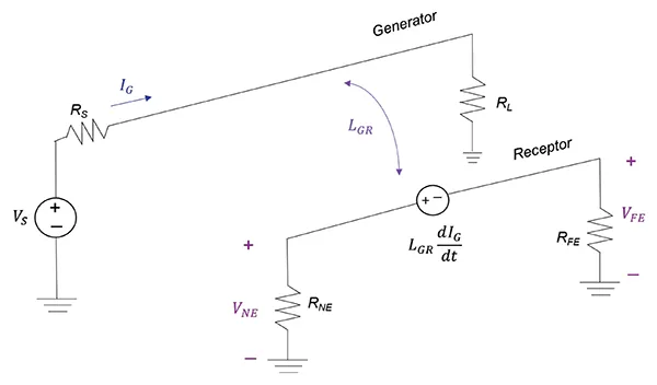
Differential pair crosstalk occurs when electromagnetic fields from one pair induce unwanted voltages or currents on a nearby victim pair, compromising signal quality. This phenomenon manifests as near-end crosstalk (NEXT), affecting the signal source, or far-end crosstalk (FEXT), impacting the receiver. Capacitive coupling dominates at lower frequencies, while inductive coupling becomes prominent at higher speeds, both contributing to noise reduction challenges. In PCB layout, unchecked crosstalk leads to bit errors, increased jitter, and reduced eye diagram margins, particularly in high-speed interfaces. Understanding these effects is vital for electric engineers designing boards for frequencies above several hundred MHz. Proper management directly supports overall signal integrity, preventing system failures in dense layouts.
The relevance intensifies with shrinking geometries and rising data rates, where trace proximity amplifies coupling risks. Industry standards like IPC-2221B emphasize conductor spacing to mitigate these issues, guiding designers toward reliable configurations. Ignoring crosstalk can cascade into electromagnetic interference (EMI) problems during compliance testing. Thus, integrating crosstalk reduction from the initial layout phase saves costly respins and accelerates time-to-market.
Fundamental Principles of Crosstalk in Differential Pairs
Crosstalk in differential pairs arises primarily from mutual capacitance and inductance between aggressor and victim traces. When signals switch rapidly, the electric field between parallel traces creates capacitive crosstalk, injecting noise proportional to the coupling coefficient. Inductive crosstalk, driven by magnetic field linkage, adds common-mode noise that differential receivers struggle to reject if unbalanced. The strength of coupling decreases exponentially with increased separation, highlighting trace spacing as a primary control factor. Engineers must model these interactions using field solver tools during pre-layout planning to predict and verify performance.
Differential signaling inherently rejects common-mode noise, but intra-pair imbalance or inter-pair proximity can convert differential crosstalk into problematic modes. For instance, odd-mode coupling affects the differential signal directly, while even-mode coupling appears as common-mode distortion. Layer transitions via vias introduce discontinuities that exacerbate coupling if not symmetric. Reference planes provide return paths that confine fields, reducing far-field coupling to adjacent layers. These principles form the foundation for all crosstalk mitigation strategies in PCB layout.
Best Practices for Trace Geometry and Spacing
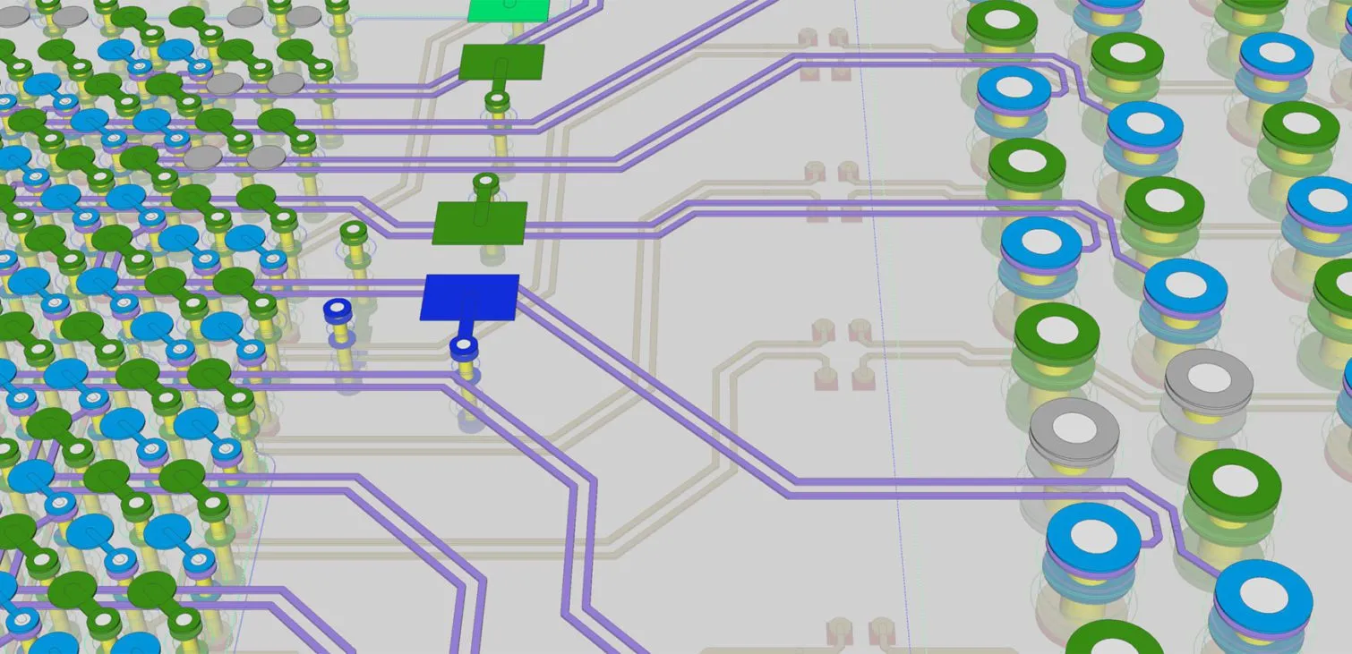
Optimal trace spacing is foundational to differential pair crosstalk reduction, with intra-pair spacing tightly controlled for characteristic impedance while inter-pair spacing widened to minimize coupling. A common guideline maintains inter-pair separation at least five times the intra-pair gap, ensuring coupling coefficients remain below acceptable thresholds. Uniform trace width and gap throughout the route preserve impedance continuity and balance, preventing mode conversion. Engineers should allocate dedicated routing channels for high-speed pairs, avoiding encroachment by unrelated signals. This structured approach enhances noise reduction without excessive board real estate usage.
In multilayer boards, staggering traces on adjacent layers reduces broadside coupling, where vertical field overlap is strongest. IPC-2221B outlines minimum spacing rules based on voltage and speed, adaptable for differential applications. Simulations confirm that doubling spacing halves NEXT, providing quantitative insight during design reviews. Consistent application across the board yields predictable signal integrity.
Length Matching and Routing Symmetry
Length matching within differential pairs equalizes propagation delays, minimizing skew that amplifies crosstalk susceptibility. Engineers route pairs with serpentine or trombone patterns for fine adjustments, ensuring total length deviation stays under 10 mils for gigabit speeds. Symmetry extends to bends, where arcs replace 90-degree corners to avoid impedance steps and unequal coupling. Maintaining pair polarity during routing prevents phase reversal, a subtle yet critical error source. These practices collectively bolster noise reduction by preserving signal balance.
Routing topology influences crosstalk; broadside coupled pairs on inner layers offer tighter coupling for lower impedance but demand precise control. Edge-coupled pairs on outer layers simplify fabrication while requiring wider spacing for isolation. Deskewing during post-route optimization refines performance, with verification via time-domain reflectometry.
Layer Stackup and Reference Plane Strategies
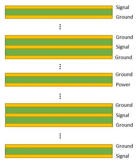
A well-defined layer stackup with dedicated ground planes adjacent to signal layers confines fields and provides low-inductance returns, slashing crosstalk by up to 20 dB. Solid reference planes under differential pairs absorb return currents, minimizing loop areas that foster inductive coupling. Splitting planes only when necessary, with stitching vias bridging gaps, maintains continuity. Orthogonal routing on adjacent signal layers aligns fields perpendicularly, further attenuating coupling. This stackup discipline is non-negotiable for high-density PCB layouts.
Power planes can serve as references if decoupled properly, but ground planes preferred for clean returns. Vias placed symmetrically around pairs preserve balance during layer changes. Compliance with IPC-6012E performance specs ensures fabricated boards match design intent for signal integrity.
Via Management and Transition Optimization
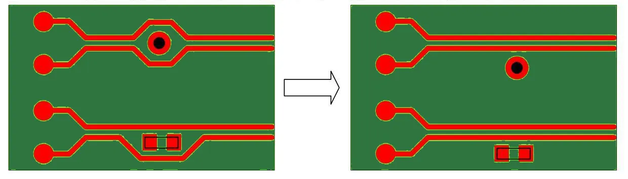
Vias introduce parasitic inductance and capacitance, hotspots for crosstalk if clustered or asymmetric. Back-drilling removes stubs to shorten via lengths, reducing reflections and coupling. Pairing vias with nearby ground vias creates shielded transitions, confining fields. Fanout patterns with minimal jogs maintain pair integrity post-BGA escape. Limiting layer changes keeps total via count low, simplifying crosstalk control.
Shielding traces between pairs, grounded via stitching, intercepts stray fields effectively. Pre-layout planning identifies via farms, allowing spacing adjustments early.
Advanced Techniques for Enhanced Noise Reduction
Guard traces or moats between sensitive pairs divert coupling currents when grounded properly. Active shielding with driven guards cancels fields proactively, suited for extreme densities. Frequency-domain analysis pinpoints resonances, guiding selective damping. Hybrid routing combines microstrip and stripline for optimized coupling profiles. These methods layer atop basics for superior performance.
Conclusion
Reducing differential pair crosstalk demands a holistic PCB layout approach, from precise trace spacing to robust reference planes and symmetric routing. Implementing these best practices ensures signal integrity, mitigates noise reduction challenges, and supports high-speed reliability. Electric engineers benefit from early simulations and standard adherence, avoiding common pitfalls. Prioritizing these techniques yields designs ready for production, minimizing iterations. Ultimately, disciplined layout elevates overall board performance.
FAQs
Q1: What role does trace spacing play in differential pair crosstalk reduction?
A1: Trace spacing directly controls capacitive and inductive coupling between differential pairs in PCB layout. Wider inter-pair spacing reduces NEXT and FEXT by lowering mutual inductance, a core noise reduction strategy. Engineers typically aim for separations several times the intra-pair gap to maintain signal integrity without excessive board area. Consistent application across layers prevents hotspots.
Q2: How do reference planes contribute to signal integrity in differential pair routing?
A2: Reference planes provide low-impedance return paths, confining electromagnetic fields and minimizing crosstalk in high-speed PCB layouts. Solid ground planes adjacent to signal layers reduce loop inductance, enhancing common-mode rejection. Stitching vias ensure continuity, preventing gaps that amplify noise. This setup aligns with standard guidelines for reliable performance.
Q3: Why is length matching critical for minimizing differential pair crosstalk?
A3: Length matching equalizes propagation delays within pairs, reducing skew that heightens crosstalk susceptibility during transitions. Unequal lengths convert differential signals to common-mode, degrading noise reduction. Precise serpentine adjustments maintain balance, preserving eye quality. Verification post-routing confirms compliance for signal integrity.
Q4: What are common via-related issues in PCB layout for crosstalk control?
A4: Asymmetric or stubbed vias disrupt pair balance, introducing discontinuities that boost coupling. Back-drilling and ground via shielding mitigate these in multilayer boards. Minimizing transitions preserves impedance continuity. Proper management ensures robust signal integrity across layers.
References
IPC-2221B — Generic Standard on Printed Board Design. IPC, 2009
IPC-6012E — Qualification and Performance Specification for Rigid Printed Boards. IPC, 2015
J-STD-001GS — Requirements for Soldered Electrical and Electronic Assemblies. IPC, 2020


