Introduction
Design for Manufacturability (DFM) represents a critical approach in PCB engineering that bridges the gap between design intent and production reality. By incorporating manufacturing constraints early in the design phase, engineers can prevent costly revisions, delays, and defects that plague PCB projects. This process ensures boards are not only functional but also producible at scale with high yield rates. For electric engineers, mastering DFM translates to reliable performance under real-world conditions while optimizing resource use. Key aspects include adhering to a design for manufacturability PCB checklist, following DFM rules for PCB assembly, and leveraging tools to spot issues proactively. Ultimately, effective DFM minimizes PCB manufacturing costs and elevates overall project success.
What Is Design for Manufacturability (DFM) and Why It Matters for PCBs
Design for Manufacturability refers to the systematic integration of fabrication and assembly constraints into the PCB layout process from the outset. It involves evaluating factors like material properties, process tolerances, and equipment limitations to create designs that align with production capabilities. In the PCB industry, DFM matters because even minor oversights can lead to yield losses exceeding 20 percent in high-volume runs, escalating costs and timelines. Electric engineers benefit from DFM by ensuring signal integrity, thermal management, and mechanical stability without compromising innovation. Standards such as IPC-2221C provide foundational guidelines for trace sizing and spacing, promoting consistency across designs. Ignoring DFM often results in common PCB manufacturing errors, underscoring its role in achieving first-pass success.
DFM extends beyond basic compliance to foster collaboration between design teams and manufacturing partners. It anticipates challenges like drill breakout or solder mask misalignment that arise during etching, plating, or reflow. By prioritizing DFM, engineers reduce scrap rates and rework, directly contributing to cost efficiency. Factory-driven insights reveal that designs passing rigorous DFM reviews experience fewer assembly defects and higher reliability in field applications. This proactive mindset aligns with industry demands for faster prototyping cycles and scalable production.
Key DFM Rules for PCB Fabrication
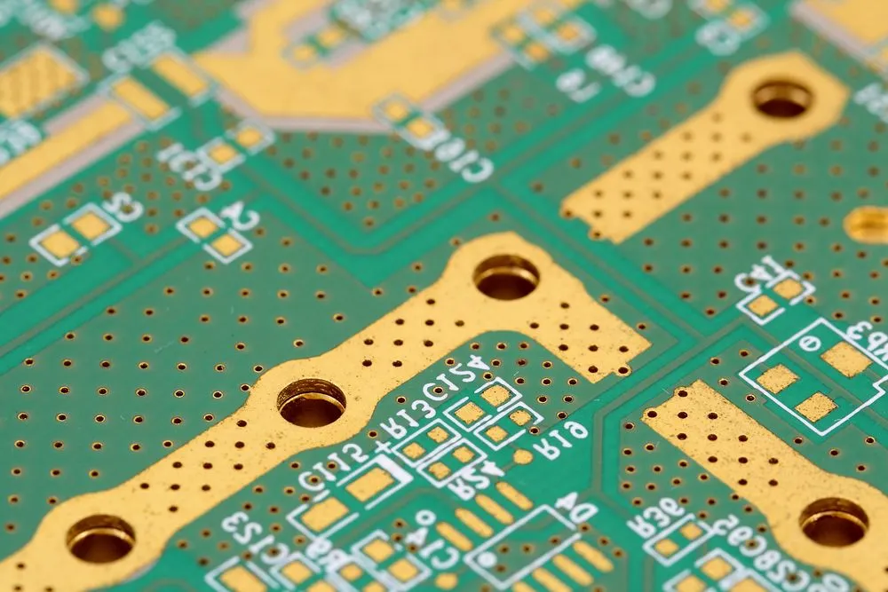
PCB fabrication begins with precise layer stackup planning to maintain symmetry and control impedance. Asymmetric stacks induce warpage due to differential thermal expansion, compromising flatness during assembly. Engineers should specify dielectric thicknesses greater than 90 micrometers between cores and use at least two plies of prepreg for stability. Copper weights for power planes often require 2 to 3 ounces to handle currents above 2 amperes, while signal layers suffice with 1 ounce. Balancing copper distribution across layers prevents uneven etching and plating stresses. Visual inspections post-fabrication confirm adherence to these principles.
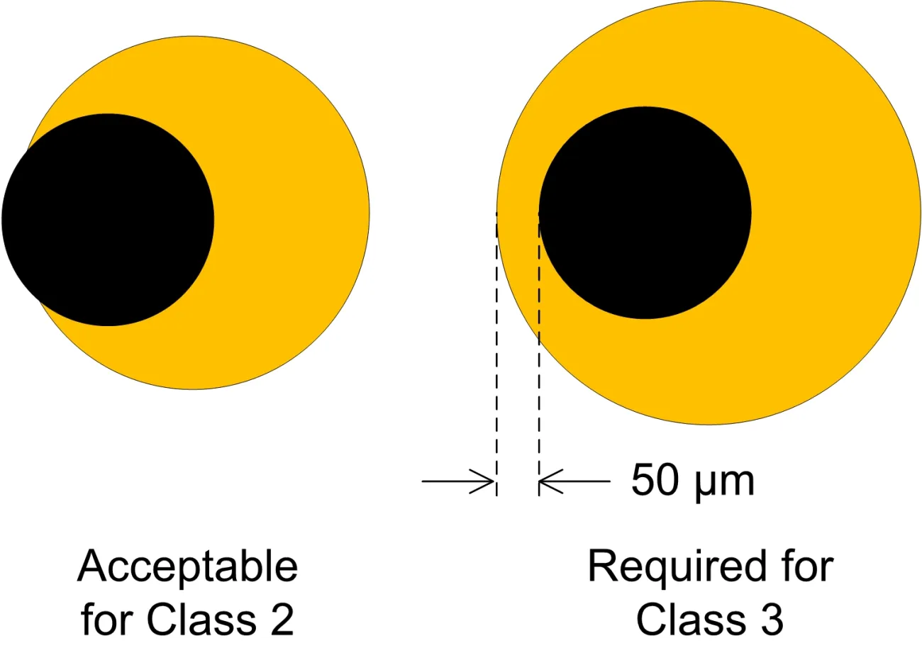
Drill design forms the backbone of interconnect reliability, demanding attention to aspect ratio, annular rings, and clearances. Through-hole aspect ratios typically stay below 10:1, calculated as board thickness divided by drill diameter, to ensure proper plating without voids. Annular rings must provide at least 2 mils externally and 1 mil internally for class 3 boards per IPC-6012F, preventing breakout during off-center drilling. Drill-to-copper clearance accounts for plating thickness, often adding 2 mils to the nominal drill size for safety. Hole-to-hole spacing exceeds 6 mils to avoid structural weakness from overlapping debris. These parameters directly impact yield, as violations lead to opens or shorts.
Trace routing demands minimum widths and spacings scaled to copper weight and voltage requirements. IPC-2221C outlines current-carrying capacity formulas, where external traces use a factor of 0.048 and internal 0.024, factoring in temperature rise. Common minimums include 5 mils for 1-ounce outer layers, increasing to 14 mils for 4-ounce. Spacing prevents arcing, with 8 mils typical for 2-ounce copper under standard voltages. Copper-to-edge clearances of 7 to 10 mils safeguard against delamination near panel borders. Acid traps, formed by acute angles in pours, trap etchant and cause undercuts, so 45-degree chamfers or teardrops resolve this.
Solder mask and silkscreen layers require defined expansions and reliefs for alignment tolerances. Solder mask clearance from pads typically exceeds 4 mils to avert bridging, with dams between fine-pitch pads at 5 mils for standard processes. Registration tolerances hover around 2 mils, necessitating expansion rules in Gerber files. Silkscreen avoids pads by 4.5 mils, copper by 6 mils, and holes by 8 mils, ensuring legibility without interference. Vias benefit from tenting or plugging to prevent solder wicking. These layers protect the board while facilitating inspection and assembly.
Suggested Reading: Optimizing Solder Paste Stencil Design for Flawless PCB Assembly
DFM Rules for PCB Assembly
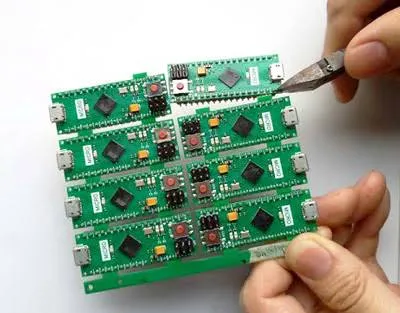
Assembly-focused DFM emphasizes component placement, fiducials, and stencil compatibility to streamline SMT and through-hole processes. Fiducials, three to four per board with 1 millimeter size and 0.2 millimeter contrast, enable precise machine alignment within 25 micrometers. Component spacing allows 5 mils between fine-pitch leads to prevent bridging during reflow. Polarization marks and reference designators remain visible post-placement, with minimum text heights of 25 mils. J-STD-001J governs solder joint criteria, requiring 75 percent barrel fill for through-holes and no cracks exceeding 10 percent pad length internally. These rules reduce defects like tombstoning or insufficient wetting.
Thermal management integrates vias under hot components, spaced 7 mils from traces in pours for reliefs. Plane splits demand 5 to 6 mils clearance around holes to isolate voltages and prevent coupling. For mixed-technology boards, segregate SMT from through-hole zones to optimize wave soldering paths. Stencil apertures match pad shapes, with home plating reduced by 5 percent for QFNs to control paste volume. Assembly panels incorporate breakaway tabs at least 10 mils wide for depaneling without stress. Adhering to these enhances yield and supports high-mix production.

Common PCB Manufacturing Errors and How to Avoid Them
Insufficient annular rings top the list of fabrication pitfalls, causing drill breakouts that sever connections. Designers mitigate this by oversizing pads beyond drill diameter plus twice the minimum ring, verified via layer-by-layer review. Slivers of isolated copper less than 4 mils wide act as antennas, inducing noise; balanced thieving patterns and minimum feature checks eliminate them. Starved thermals with voids hinder heat flow, resolved by spoke widths exceeding 7 mils or via arrays. Floating copper fragments short planes, caught by connectivity netlists against Gerbers.
Acid traps and mouse bites from sharp corners erode traces unevenly, preventable with 45-degree filleting and smooth pours. Copper too near edges risks interlayer shorts, maintained at 10 mils minimum. Solder mask overlaps expose pads or bridge fine features, addressed through precise expansion in design rules. Silkscreen printing over vias obscures inspection, avoided by clearance enforcement. Stubbed vias unconnected to layers waste drill cycles; stackup views confirm tenting. Early DFM software analysis flags these, slashing respin rates.
Suggested Reading: Drill Hole Considerations for PCB DFM: Avoiding Common Manufacturing Errors
Minimizing PCB Manufacturing Costs Through DFM
Cost optimization starts with standard board dimensions and layer counts, as custom sizes inflate tooling expenses. Panelization maximizes yield by arraying multiples with 15-mil V-scores or tab-rout spacing. Fewer vias and blind/buried types reduce drill setups, while through-holes favor economy. Standard hole sizes cluster around 0.2 to 1 millimeter to share bits. Thicker copper demands longer etch times, so 1-ounce suffices unless currents dictate otherwise. These choices cut per-unit costs by streamlining processes.
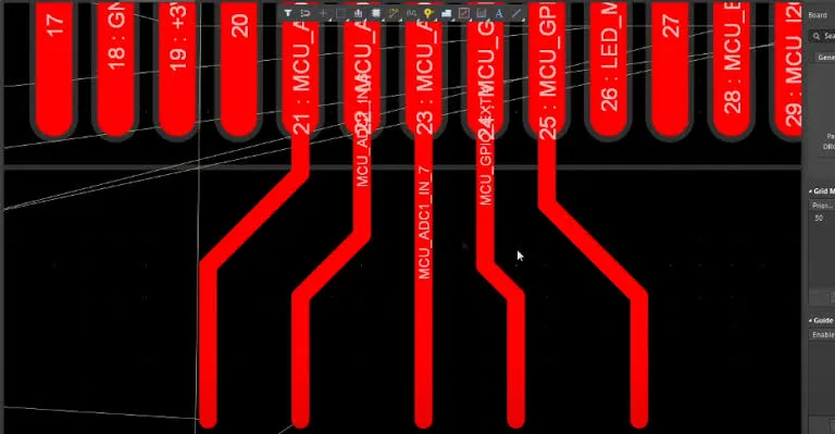
DFM software tools play a pivotal role, integrating design rule checks (DRC) with fabrication simulations. Standalone analyzers scan Gerbers for slivers, annular violations, and mask alignments, generating reports pre-submission. EDA-embedded modules enforce min/max constraints iteratively during routing. Cloud-based options provide instant feedback on stackup warpage or impedance mismatches. Leveraging these tools prevents errors that add 20 to 50 percent to budgets via rework. Factory insights confirm DFM-optimized designs yield 95 percent first-pass rates.
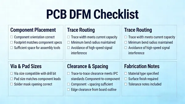
Design for Manufacturability PCB Checklist
A robust design for manufacturability PCB checklist ensures comprehensive coverage. Review drill layers for minimum sizes above 6 mils, aspect ratios under 10:1, drill-to-copper over 6 mils, annular rings per class, via-in-pad specs, complete files, and hole spacing beyond 6 mils. Signal layers demand trace widths per current, spacings for voltage, edge clearances of 10 mils, no acid traps, slivers over 4 mils, and intact thermals. Power planes verify hole clearances, split isolations, balanced thieving, and thermal via arrays.
Solder mask checks include expansion over 4 mils, dam widths at 5 mils, via tenting rules, and pad definitions. Silkscreen confirms pad clearances, line widths over 4 mils, visible designators, and markings. General items cover netlist matches, stackup symmetry, fiducials, and fab notes. Run this pre-tapeout to align with capabilities.
Conclusion
DFM demystified empowers electric engineers to craft PCBs that excel in production and performance. Core principles like annular integrity, trace compliance, and assembly fiducials form a solid foundation. Integrating checklists and software tools averts common errors while slashing costs. Standards such as IPC-6012F and J-STD-001J anchor these practices in proven reliability. Prioritizing DFM yields efficient, defect-free boards ready for demanding applications. Embrace it for seamless transitions from concept to volume manufacturing.
FAQs
Q1: What is a design for manufacturability PCB checklist?
A1: A design for manufacturability PCB checklist verifies critical parameters like drill clearances, trace spacings, annular rings, and mask expansions before fabrication. It categorizes checks across drill, signal, power, solder mask, and silkscreen layers to catch issues early. Factory-driven reviews using this list ensure compliance with capabilities, reducing respins. Typical items include aspect ratios under 10:1 and edge clearances over 10 mils. This tool streamlines workflows for electric engineers targeting high yields.
Q2: What are essential DFM rules for PCB assembly?
A2: DFM rules for PCB assembly prioritize fiducial placement, component spacing over 5 mils for fine-pitch, and stencil apertures matching pads. Thermal vias under components aid reflow, while J-STD-001J dictates joint fills at 75 percent. Segregate SMT and through-hole zones to optimize soldering. Visible polarity marks and netlist-verified placements prevent misalignment. These rules minimize bridging and tombstoning in production.
Q3: How can engineers avoid common PCB manufacturing errors?
A3: Common PCB manufacturing errors like annular ring breakouts, copper slivers, and acid traps stem from inadequate clearances and sharp features. Avoid them by enforcing 6-mil drill-to-copper, 4-mil minimum slivers, and 45-degree filleting. Netlist comparisons detect stubs, while balanced pours prevent starved thermals. Iterative DRC runs flag violations early. This proactive stance aligns with IPC-2221C for robust designs.
Q4: What role do DFM software tools play in minimizing PCB manufacturing costs?
A4: DFM software tools analyze Gerbers for violations like mask overlaps or impedance drifts, simulating warpage and yield. Integrated DRC enforces rules during design, while standalone platforms report fixes pre-submission. They enable panel optimization and standard feature use, cutting tooling by 20 to 30 percent. Electric engineers gain factory-aligned insights without respins. These tools transform DFM into a cost-saving powerhouse.
References
IPC-2221C — Generic Standard on Printed Board Design. IPC, 2023
IPC-6012F — Qualification and Performance Specification for Rigid Printed Boards. IPC, 2023
J-STD-001J — Requirements for Soldered Electrical and Electronic Assemblies. IPC, 2024