Introduction
Electronic hobbyists frequently encounter projects that demand more power than standard circuit boards can handle, such as driving motors, high-power LEDs, or custom power supplies. A DIY high-current PCB offers the flexibility to tailor your board exactly to your needs, avoiding the limitations of off-the-shelf options. This guide walks you through the essentials of designing, etching, and assembling high-current boards at home. You will learn practical steps to ensure reliability and safety while incorporating key techniques like etching high-current traces and soldering thick copper PCBs. By following these structured approaches, hobbyists can power ambitious projects without compromising performance. The focus remains on accessible methods using common tools and materials.
What Are High-Current PCBs and Why They Matter for DIY Projects
High-current PCBs feature traces and planes capable of carrying substantial electrical loads without excessive heating or failure. In hobbyist applications, these boards support devices like battery chargers, motor drivers, and amplifiers that exceed the typical 1-2 ampere limits of standard single-ounce copper boards. The relevance stems from the growing popularity of DIY electronics, where compact, efficient power delivery enhances project portability and performance. Without proper high-current design, traces can overheat, leading to delamination or fire risks during operation. Hobbyists benefit from DIY high-current PCBs because they enable experimentation with real-world power levels in garage workshops. Adhering to industry guidelines ensures these homemade boards meet basic reliability standards.
Key Technical Principles for High-Current PCB Design
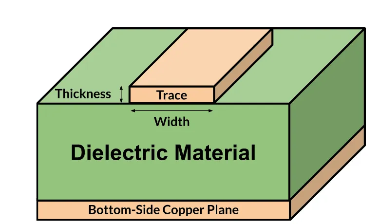
Designing a DIY high-current PCB starts with understanding copper thickness and trace geometry. Standard boards use one-ounce copper, equivalent to about 35 microns thick, but high-current applications require two-ounce or heavier foils to reduce resistance and heat buildup. Wider traces distribute current more evenly, minimizing voltage drop across the board. Thermal management plays a critical role, as elevated temperatures can degrade solder joints and insulation over time. According to IPC-2221, generic standard on printed board design, trace dimensions must account for allowable temperature rise based on ambient conditions and layer position.[[1]](https://www.protoexpress.com/blog/ipc-2221-circuit-board-design) External layers dissipate heat better than internal ones, influencing layout choices. Hobbyists should prioritize outer-layer routing for power paths whenever possible.
Another principle involves via usage and plane pours. Multiple vias in parallel increase current capacity through thermal vias or filled designs, aiding heat transfer to other layers. Solid copper pours act as low-impedance returns and heat spreaders, but they demand careful etching to avoid undercuts. Layer stackup affects overall performance, with multilayers offering redundancy for extreme currents. Ground planes reduce electromagnetic interference, essential for stable hobbyist power circuits. Balancing these elements prevents hotspots and ensures long-term durability.
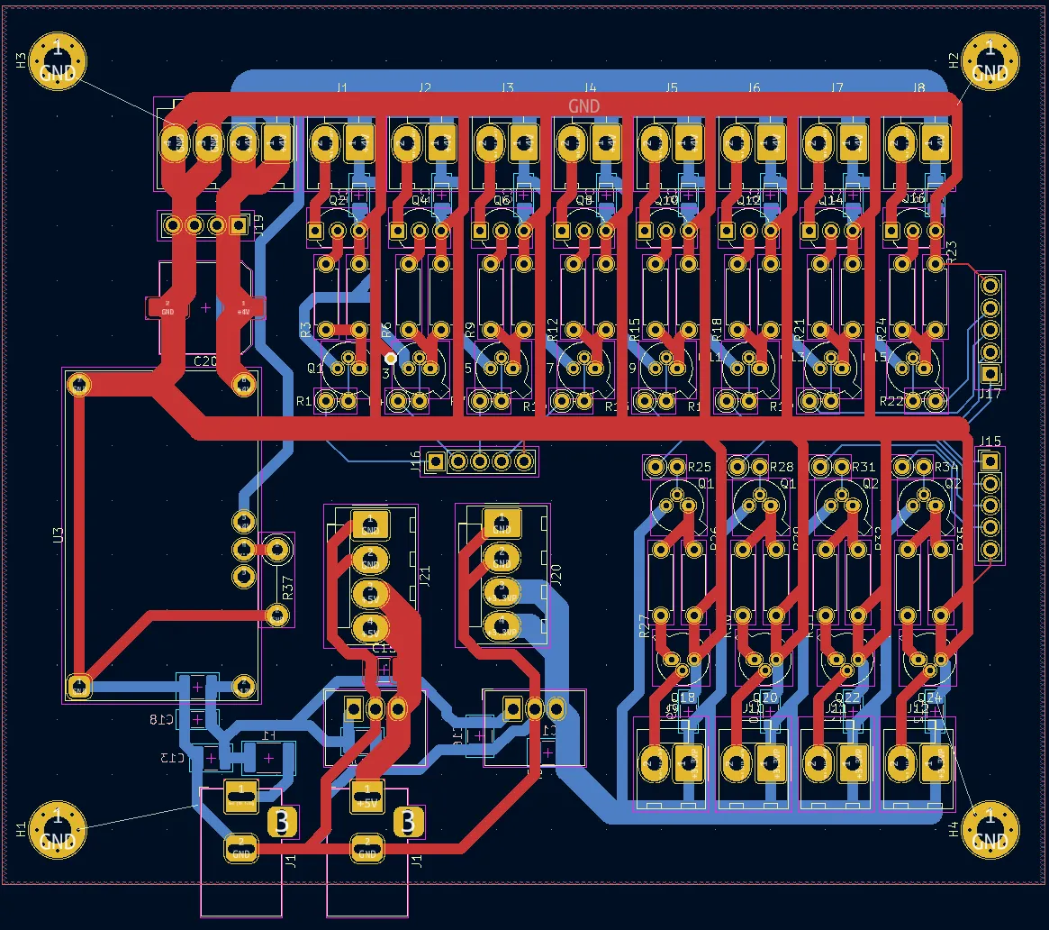
Selecting PCB Design Software for Hobbyists
PCB design software for hobbyists simplifies the transition from schematic to Gerber files ready for home etching. Look for tools with built-in trace width calculators that follow established standards, helping compute dimensions based on current, copper weight, and temperature rise. These programs often include 3D previews to visualize board thickness and component fit. Free versions support essential features like autorouting and DRC checks, crucial for high-current layouts. Hobbyists appreciate intuitive interfaces that handle differential pairs and power planes without steep learning curves. Exporting to formats like PDF or image for toner transfer makes home fabrication straightforward.
Etching High-Current Traces at Home
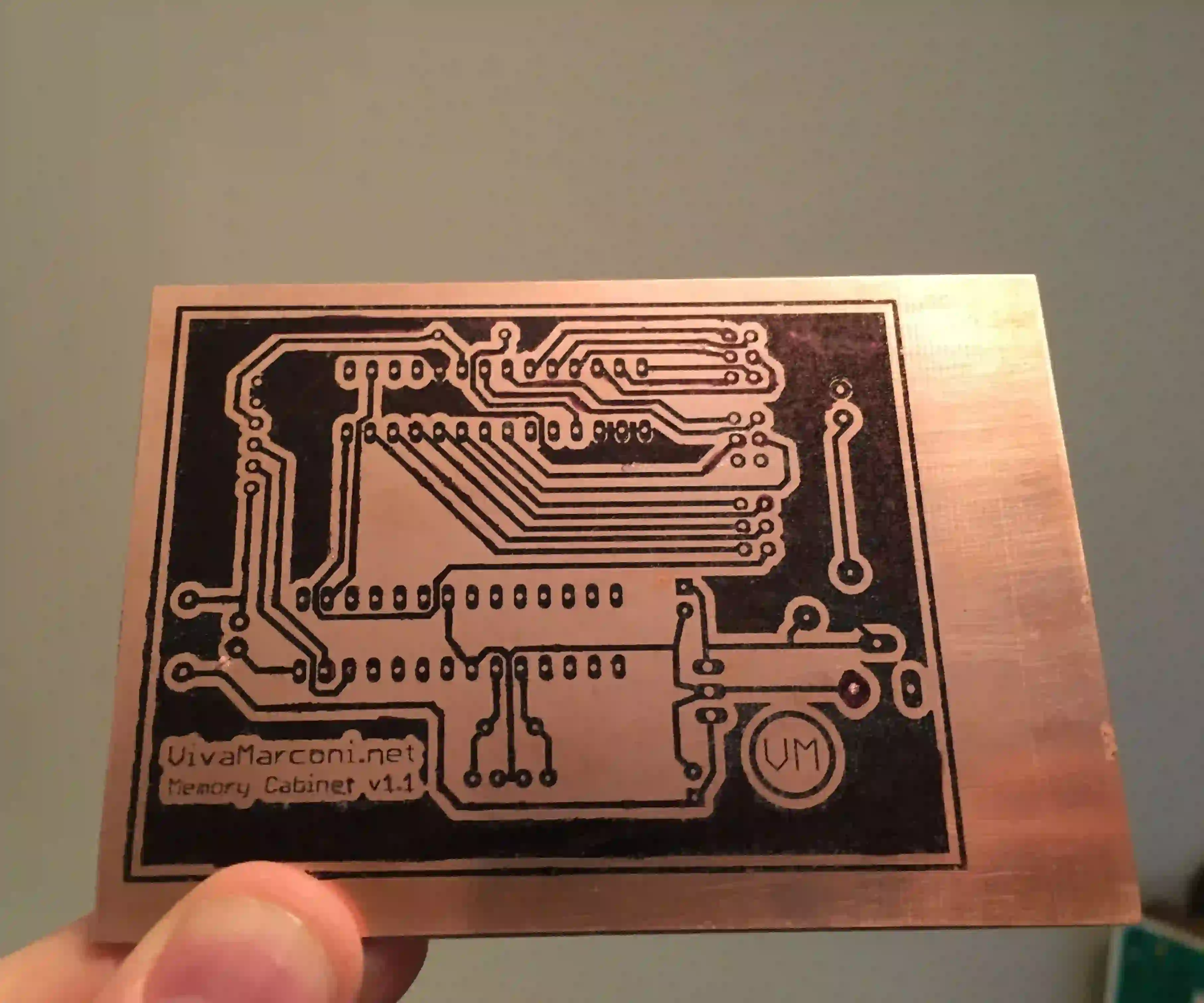
Etching high-current traces requires adjustments for thicker copper, as standard etchants work slower on two-ounce foils. Begin with a clean copper-clad board, applying resist via toner transfer or dry film photoresist for sharp edges. Ferric chloride or persulfate solutions etch effectively, but agitate vigorously and warm the bath to penetrate deeper copper layers. Etch times double or triple compared to thin foils, so monitor closely to prevent over-etching narrow sections. After etching, neutralize residues thoroughly to avoid corrosion in power paths. This process yields robust DIY high-current PCBs capable of handling hobbyist loads.
Common challenges include undercut edges on wide traces, mitigated by fresher etchant and bubble agitation. For complex designs, panelize multiple boards to optimize bath usage. Post-etch tinning with solder preserves copper from oxidation during storage. Test continuity with a multimeter before assembly. Patience in this step ensures traces meet design specs without bridging or thinning.
Soldering Thick Copper PCBs: Practical Tips
Soldering thick copper PCBs demands more heat input due to the copper's thermal mass acting as a heat sink. Use a temperature-controlled iron set above 350 degrees Celsius with a chisel tip for broad contact. Apply ample flux to improve wetting, as thick copper resists solder flow without activation. Preheat the board in an oven or with hot air to equalize temperatures and prevent warping. For through-hole components, tin leads first to avoid cold joints. Wave soldering mimics professional results but requires setup beyond basic hobbyist tools.
Troubleshooting lift-offs involves thermal relief pads in design, connecting traces to pads with narrow necks. Hot air stations excel for surface-mount parts on heavy copper, allowing uniform heating. Clean flux residues post-soldering to prevent dendritic growth under voltage. Inspect joints visually and with continuity tests for reliability. These techniques make soldering thick copper PCBs accessible for home builders.
Building a Power Supply PCB at Home: A Step-by-Step Example
Start building a power supply PCB at home by sketching a simple regulator circuit with input filtering and output capacitors. In PCB design software for hobbyists, route wide traces from the rectifier to load points, incorporating fuses for safety. Generate toner-compatible prints, transfer to two-ounce copper board, and etch as described. Drill holes precisely for heatsinks and connectors, then solder components starting with low-profile ones. Add conformal coating over exposed traces for humidity protection. Bench-test with dummy loads to verify no hotspots.
This example demonstrates scalability for hobbyist needs, like 12-volt supplies for robotics. Iterate designs based on thermal imaging if available, or finger tests for heat. Document changes for future revisions. Such projects build confidence in handling real power safely.
Best Practices and Troubleshooting for DIY High-Current PCBs
Follow IPC-A-600 acceptability criteria for visual inspection of etched traces, ensuring no voids or lifts.[[2]](https://www.facebook.com/groups/2259899699/posts/10156506497034700) Incorporate test points for in-circuit measurements during prototyping. Use FR4 laminate rated for your voltage, avoiding exotics for cost. Safety first: isolate high-voltage sections and add isolation slots. Common pitfalls like insufficient trace width cause failures, addressed by iterative calculations. Multilayer DIY via press-fit pins expands options for complex power distribution.
For troubleshooting, measure resistance and temperature rise under load. Reflow issues on thick copper stem from poor preheat, fixed by profiled ovens. Sustainable practices include recycling etchant where possible. These habits elevate hobbyist boards to professional standards.
Conclusion
DIY high-current PCBs empower hobbyists to tackle power-hungry projects with custom reliability. From design principles guided by IPC-2221 to hands-on etching and soldering, each step builds capability. Key takeaways include prioritizing thick copper, wide traces, and thermal awareness for safe operation. Experiment iteratively, always testing under realistic loads. This approach not only powers your creations but fosters deeper electronics understanding. Start small, scale confidently.
FAQs
Q1: What copper thickness should hobbyists use for a DIY high-current PCB?
A1: For DIY high-current PCBs, two-ounce copper balances etchability and current capacity for most hobbyist projects up to moderate power levels. Thicker foils like three-ounce suit extreme loads but complicate home etching due to longer times. Reference IPC-2221 for sizing based on expected current and temperature rise. Always verify with thermal tests post-assembly. This ensures reliable performance without professional equipment.
Q2: How do you etch high-current traces at home effectively?
A2: Etching high-current traces involves using fresh etchant and mechanical agitation to handle thick copper evenly. Toner transfer works well for sharp definition on wide paths. Warm the solution to 40-50 degrees Celsius for faster action, monitoring to avoid undercuts. Rinse and tin immediately after. This method produces durable traces for power applications in hobbyist setups.
Q3: What are tips for soldering thick copper PCBs as a beginner?
A3: Soldering thick copper PCBs requires a high-wattage iron, abundant flux, and preheating to overcome heat sinking. Chisel tips aid broad joints, while hot air handles SMD parts. Tin components separately for easier flow. Inspect for full wetting and fillet formation per J-STD-001 guidelines. Practice on scraps builds skill for flawless assemblies.
Q3: Which PCB design software for hobbyists supports high-current features?
A3: PCB design software for hobbyists with trace calculators and plane tools excels for high-current layouts. Free options offer DRC for clearance and width checks aligned with standards. 3D views help assess heatsink fit. Export directly for home etching. These tools make professional-grade DIY high-current PCBs achievable without cost.
References
IPC-2221 — Generic Standard on Printed Board Design. IPC
IPC-A-600K — Acceptability of Printed Boards. IPC
IPC-6012E — Qualification and Performance Specification for Rigid Printed Boards. IPC
J-STD-001H — Requirements for Soldered Electrical and Electronic Assemblies. IPC


