Introduction
Electronic hobbyists often reach a point where single-layer boards limit project complexity, pushing them toward multilayer designs. Vias serve as the essential bridges between copper layers, enabling compact routing and higher functionality in homemade PCBs. Creating these connections at home requires ingenuity, as professional plating equipment is unavailable. This article explores practical DIY via drilling techniques, homemade PCB vias methods, and simple via plating approaches suitable for low-cost via creation. By understanding basic principles and hands-on steps, hobbyists can achieve reliable interlayer connections without sending boards to a fab. These methods balance accessibility with performance for prototype builds.
What Are PCB Vias and Why Do They Matter for DIY Projects?
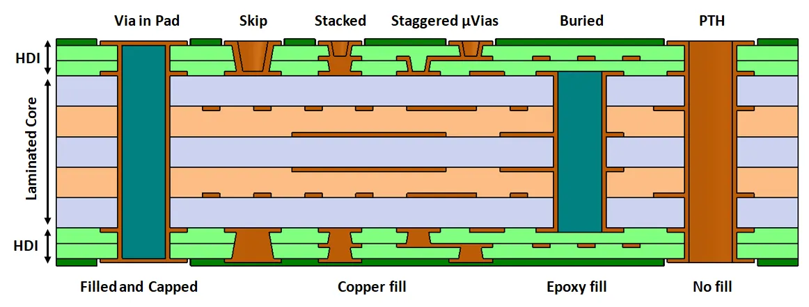
A via is a small hole that provides electrical continuity between different layers of a printed circuit board. In multilayer PCBs, vias allow signals, power, and ground to transition vertically, freeing up surface space for components and traces. For hobbyists, mastering homemade PCB vias unlocks advanced projects like audio amplifiers or sensor arrays that demand dense layouts. Without proper vias, connecting PCB layers at home becomes cumbersome, often leading to bulky wire jumpers or unreliable hacks. Industry standards like IPC-4761 classify via protection types, from tented to filled, guiding even DIY efforts toward durability. Reliable vias reduce signal integrity issues and mechanical stress in home-fabricated boards.
Through-hole vias penetrate all layers, while blind and buried vias connect only specific ones, though the latter are challenging for home setups. Hobbyists typically focus on through-hole types due to simpler DIY via drilling. These vias must withstand soldering temperatures and vibrations common in prototypes. Poorly made vias can cause open circuits or shorts, derailing projects. Adhering to principles from IPC-6012 ensures minimum plating thickness and annular ring sizes, even in rudimentary forms. This foundation matters for hobbyists scaling from perfboards to custom multilayers.
Technical Principles Behind PCB Vias
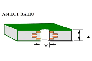
Vias function by plating the drilled hole walls with conductive material, typically copper, to form a barrel connecting pads on inner and outer layers. The aspect ratio, defined as board thickness divided by hole diameter, affects plating quality; ratios above 10:1 risk voids in professional processes and are impractical at home. Clean drilling removes debris that could insulate walls, while plating deposits a uniform layer for low resistance. Mechanical stress from thermal expansion demands robust barrels to prevent cracking. Standards like IPC-A-600 outline acceptability criteria for via plating continuity and appearance. Understanding these ensures DIY methods mimic factory reliability.
Plating involves electroless copper deposition followed by electrolytic thickening in fabs, but hobbyists adapt with conductive inks or solders. Hole wall preparation activates surfaces for adhesion, preventing delamination. Current carrying capacity depends on barrel cross-section; smaller vias suit signals, larger ones power. Aspect ratios under 5:1 work best for low-cost via creation at home. IPC-6012 specifies minimum copper thickness in vias, around 20 microns for class 2 boards, informing homemade targets. These principles guide safe current limits and longevity in prototypes.
Practical DIY Methods for Homemade PCB Vias
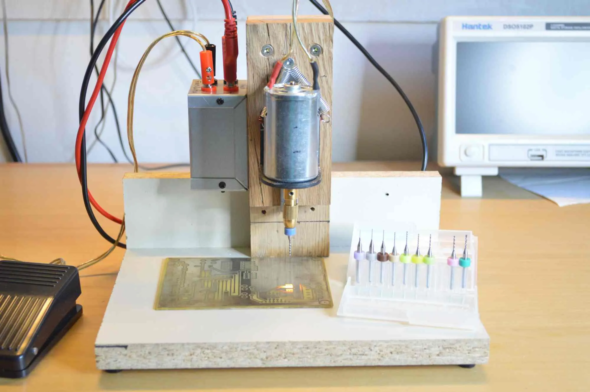
DIY via drilling starts with precise tools like a Dremel or hand drill fitted with carbide bits sized 0.5 to 1 mm for typical hobby boards. Mark via locations using a plotted film or CNC if available, then drill slowly to avoid heat buildup that warps FR4 substrate. Clean holes with isopropyl alcohol and a brush to expose fresh epoxy for better adhesion. Common mechanical methods include inserting tinned wire snippets, soldering top and bottom pads to form a robust connection. This approach excels for low-cost via creation, offering high current capacity without chemicals. Rivets or hollow brass tubes pressed into place provide similar results, flaring ends for retention.
For simple via plating, apply conductive silver ink pens inside drilled holes, bridging layers after curing. Wipe excess ink from pads, then tin with fluxed solder for protection. This method suits signal vias under 100 mA, though resistance is higher than plated copper. Test continuity with a multimeter before assembly. More advanced hobbyists attempt DIY electroless plating by seeding walls with graphite spray, followed by copper sulfate and battery electrolysis. Monitor plating time to achieve even coverage, rinsing thoroughly to halt the reaction. These techniques enable connecting PCB layers at home with minimal investment.
Step-by-Step Guide to Low-Cost Via Creation at Home
Begin by designing your multilayer stackup, typically two or four layers using pre-sensitized boards or double-sided copper clad. Etch outer layers first, align inner ones with registration holes, then laminate under vacuum bag and oven cure at controlled temperatures. Drill vias post-lamination using a fixture for alignment, starting with pilot holes if board thickness exceeds 1.6 mm. For wire vias, cut 22 AWG wire to length, insert through holes, and solder both ends while clamping to prevent movement. File excess wire flush, then apply solder mask if desired for insulation.
Conductive paste methods involve filling holes with epoxy mixed with copper powder or commercial via fill pastes, then curing and soldering over. Vacuum assist removes air bubbles for solid fills. For plating emulation, swab walls with palladium activator if available, or use constant-current electrolysis with vinegar-copper solutions. Plate for 30-60 minutes, inspecting for uniform shine. Buff and tin final barrels. Always bake boards post-process to outgas moisture, mimicking IPC-6012 reliability tests. This workflow yields functional homemade PCB vias for hobby prototypes.
Best Practices and Troubleshooting for DIY Vias
Maintain drill speeds under 2000 RPM to minimize fiberglass fuzz that blocks plating. Use lubricants like ethanol for smoother cuts. Fixture boards rigidly to prevent wandering bits. After any method, perform thermal shock tests by cycling through reflow profiles to verify integrity. Inspect under magnification for cracks or lifts per IPC-A-600 guidelines. Space vias at least 0.5 mm apart to avoid crosstalk in high-speed signals.
Common pitfalls include misalignment from poor registration, fixed by fiducial marks. Weak connections arise from oxidized walls; always abrade and clean immediately. Over-drilling enlarges holes, reducing annular ring below standards, so measure bits accurately. For plated attempts, uneven current causes knobby deposits; agitate solutions gently. Mechanical vias may loosen under vibration; secure with epoxy fillets. Document iterations to refine processes for future boards.
Conclusion
DIY PCB vias empower electronic hobbyists to build sophisticated multilayer boards at home using accessible tools and materials. From basic wire insertions to conductive inks and rudimentary plating, these methods deliver reliable connections without factory costs. Adhering to principles like aspect ratios and cleanliness ensures performance akin to standards. Experiment iteratively, prioritizing safety with ventilation for chemicals. As skills grow, low-cost via creation becomes routine, expanding project possibilities. Hobbyists gain independence, prototyping faster toward innovation.
FAQs
Q1: What is DIY via drilling and how do I start at home?
A1: DIY via drilling involves using a precision drill to create holes through multilayer PCB stacks for interlayer connections. Secure the board in a fixture, select carbide bits matching your design diameters, and drill at low speeds to avoid damage. Clean debris thoroughly afterward. This foundational step enables all homemade PCB vias methods, ensuring alignment for subsequent plating or filling. Practice on scrap to perfect technique.
Q2: How can I achieve simple via plating for connecting PCB layers at home?
A2: Simple via plating uses conductive pens or pastes swabbed into drilled holes, cured, then soldered for contact. For enhanced conductivity, seed with graphite and electrolyze copper from household solutions. Maintain even coverage by rotating boards during plating. This low-cost approach suits signals and power in hobby prototypes, mimicking electroless processes. Test resistance post-process for reliability.
Q3: What are the best low-cost methods for homemade PCB vias?
A3: Low-cost via creation favors mechanical inserts like tinned wires or rivets soldered in place, requiring only basic tools. Conductive inks offer plated-like results without baths. Avoid complex chemistries initially to minimize failures. These techniques handle typical hobby currents while keeping expenses under a few dollars per board. Scale up as confidence builds.
Q4: Why do DIY vias sometimes fail, and how to fix them?
A4: Failures stem from poor cleaning, misalignment, or thermal stress cracking barrels. Clean holes meticulously and use fixtures for precision. Strengthen with epoxy or thicker wires for mechanics. Inspect per acceptability criteria to catch issues early. Iterative testing refines processes for durable connections in home projects.
References
IPC-6012E — Qualification and Performance Specification for Rigid Printed Boards. IPC, 2017
IPC-4761 — Design and Qualification of Printed Boards with Via Protection. IPC, 2007
IPC-A-600K — Acceptability of Printed Boards. IPC, 2020


