Introduction
Copper pours serve as essential elements in modern PCB layouts, providing ground planes, thermal relief, and improved current distribution. However, when these pours remain unconnected to any net, they become floating copper pours that introduce subtle yet significant risks. Electric engineers often encounter these issues during signal integrity simulations or EMI compliance testing. Unconnected copper pours can transform into unintended antennas, amplifying noise and degrading overall board performance. This article explores the mechanisms behind floating copper pours, their impact on PCB designs, and structured strategies to eliminate them. Understanding these principles ensures robust, reliable circuits aligned with engineering best practices.
What Is a Floating Copper Pour?
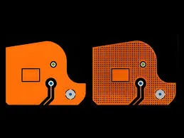
A floating copper pour refers to any area of copper plating on a PCB layer that lacks electrical connection to a defined net, such as ground or power. These regions typically arise during layout when unused board space receives a pour, but designers forget to assign thermals, vias, or traces for connectivity. In contrast, connected pours integrate seamlessly into the netlist, contributing to shielding and heat dissipation. Floating pours, however, float electrically isolated, susceptible to capacitive and inductive coupling from nearby signals. Engineers identify them in design rule checks as islands without net assignments. Recognizing this distinction proves critical for maintaining design integrity from schematic to fabrication.
Why Floating Copper Pours Matter in PCB Design
Floating copper pours compromise signal integrity by acting as parasitic elements that couple noise into sensitive traces. In high-speed designs, even small unconnected areas can resonate at operational frequencies, exacerbating crosstalk and reflections. Compliance with industry standards like IPC-2221 becomes challenging when these pours introduce uncontrolled impedance variations. Manufacturing yields suffer too, as floating regions may accumulate residues or cause solder inconsistencies during assembly. For electric engineers optimizing multilayer boards, addressing unconnected copper pours early prevents costly respins and field failures. Prioritizing connectivity transforms potential liabilities into performance enhancers.
The PCB antenna effect occurs when floating copper pours resonate with incident electromagnetic fields, much like a dedicated antenna structure. Dimensions of the pour determine its resonant frequency, often aligning with clock harmonics in digital circuits. For instance, a pour spanning a quarter-wavelength at 1 GHz behaves as a monopole, efficiently receiving or radiating energy. This coupling injects noise into adjacent signals, violating signal integrity margins. Simulations reveal voltage spikes on floating pours exceeding 100 mV peak-to-peak from nearby switching. Engineers mitigate this by ensuring all copper ties to reference planes, avoiding inadvertent RF vulnerabilities.
The PCB Antenna Effect from Unconnected Copper Pours
Unconnected pours exhibit broadband reception due to their irregular shapes, which support multiple modes. Inductive loops within the pour amplify magnetic fields from return currents in ground traces. Capacitive parasitics form between the pour and overlying components or traces, further broadening susceptibility. In multilayer stacks, via transitions exacerbate the effect if inner layers host isolated copper. Logical design reviews flag these as high-risk features during pre-layout analysis. Consistent net assignment prevents the antenna effect from undermining EMI performance.
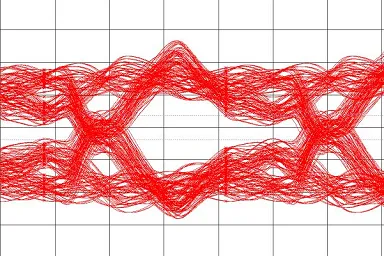
Copper Pour Noise and Its Impact on Signal Integrity
Copper pour noise arises primarily from floating regions capacitively coupling to high dv/dt nodes, such as data lines or power switches. This induced voltage modulates the pour potential, injecting common-mode noise into victim traces via mutual capacitance. Signal integrity suffers through eye diagram closure, increased jitter, and bit error rates in serial links. In power distribution networks, unconnected pours disrupt return paths, elevating PDN impedance at mid-frequencies. Engineers observe this in time-domain reflectometry as unexpected ringing. Ground referencing all pours restores low-impedance paths, stabilizing signals across the board.
Dynamic coupling intensifies during transients, where fast edges on aggressor lines excite the floating pour. The pour then re-radiates noise, affecting distant receivers through air or substrate propagation. For mixed-signal boards, this noise bridges analog and digital domains, corrupting precision measurements. Compliance testing per relevant standards highlights failures traceable to copper pour noise. Structured stitching eliminates these paths, ensuring clean signal propagation. Proactive DRC rules automate detection, streamlining the design flow.
Best Practices for Managing Copper Pours in PCB Layout
Always assign pours to ground or power nets during polygon creation to prevent floating copper. Use thermal reliefs for vias connecting components, ensuring robust solder joints without stressing copper. Stitch pours with via fences spaced at lambda/20 for RF control, maintaining return path continuity. Adhere to IPC-2221 spacing rules between pours and high-voltage traces to avoid arcing risks. Clearance settings in the layout tool should exceed minimums by 20% for safety margins. These steps yield low-noise, thermally efficient boards.
Partition pours by function: dedicate inner layers to solid ground planes, while surface pours support localized shielding. Avoid splitting pours under sensitive ICs unless isolation serves a purpose, then connect remnants explicitly. Simulate PDN impedance post-pour to verify improvements. For high-density interconnects, use hatched pours to balance copper density without excess weight. Regular connectivity checks catch orphans before Gerber output. This methodical approach aligns with engineering rigor for production-ready designs.
Troubleshooting Floating Copper Issues in Existing Designs
Inspect Gerbers for unconnected islands using polygon netlist reports from your layout software. If discovered post-fabrication, analyze noise spectra with a near-field probe to correlate peaks with pour locations. Rework involves selective etching or adding jumpers, though redesign proves preferable for volume. Signal integrity tools quantify degradation via S-parameter extraction, pinpointing coupling coefficients. In legacy boards, conformal coating suppresses some effects, but root causes demand addressing. Document findings to refine future DRC decks.
Common pitfalls include pours overlapping split planes without barriers, creating unintended bridges. Review stackup symmetry to ensure pours do not float between layers. Assembly per J-STD-001 standards flags anomalies like floating solder balls from unconnected copper. Iterative testing with spectrum analyzers confirms resolutions. Engineers build checklists incorporating these diagnostics for repeatable success.
Conclusion
Floating copper pours represent a subtle threat in PCB design, manifesting as the PCB antenna effect and copper pour noise that erode signal integrity. Connected pours, properly stitched and net-assigned, deliver shielding, thermal benefits, and PDN stability. Electric engineers benefit from logical workflows emphasizing DRC, simulation, and standards compliance like IPC-2221. Eliminating unconnected copper ensures EMI resilience and high yields. Adopt these practices to elevate design quality, avoiding respins and performance shortfalls. Robust layouts stem from vigilant copper management.
FAQs
Q1: What causes the PCB antenna effect in floating copper pours?
A1: Floating copper pours resonate at frequencies matching their dimensions, coupling electromagnetically to nearby signals. This turns isolated copper into efficient radiators or receivers, injecting noise and degrading signal integrity. Connect all pours to ground nets with stitching vias to break resonances. Simulations confirm quarter-wave lengths align with common harmonics, underscoring the need for proactive checks.
Q2: How does unconnected copper pour affect signal integrity?
A2: Unconnected copper pour capacitively couples to switching nodes, inducing voltages that propagate as common-mode noise. This raises jitter, closes eye diagrams, and elevates bit error rates in high-speed links. Tying pours to reference planes lowers PDN impedance, restoring clean signals. Time-domain analysis reveals ringing absent in connected designs.
Q3: What are best practices to avoid floating copper pour issues?
A3: Assign all copper pours to defined nets during layout, using thermal vias for connectivity. Implement stitching at close intervals for RF shielding and noise suppression. Verify with connectivity DRCs before fabrication. This prevents antenna effects and ensures compliance with design standards. Hatched patterns balance density where solids prove impractical.
Q4: Can copper pour noise from floating areas cause EMI failures?
A4: Yes, floating pours re-radiate coupled noise, failing radiated emissions tests. Broadband susceptibility amplifies harmonics from digital clocks. Ground pours provide shielding, containing fields effectively. Near-field probing isolates culprits for targeted fixes. Consistent practices yield compliant boards without iterations.
References
IPC-2221B — Generic Standard on Printed Board Design. IPC, 2003
IPC-6012E — Qualification and Performance Specification for Rigid Printed Boards. IPC, 2017
J-STD-001G — Requirements for Soldered Electrical and Electronic Assemblies. IPC, 2017


