Introduction
Transforming an initial circuit concept into a functional prototype marks a critical phase in electronics development. PCB schematic tools serve as the foundational bridge in this process, enabling engineers to visualize and refine designs before physical fabrication. These circuit design tools streamline PCB prototyping by capturing electrical connections, component placements, and signal flows in a digital format. Rapid prototyping benefits immensely from their precision, reducing iteration cycles and minimizing errors that could arise in later stages. For electric engineers, mastering schematic tools accelerates the journey from idea to reality, ensuring designs meet performance and manufacturability requirements. This article explores their pivotal role, technical underpinnings, and best practices in electronics prototyping.
What Are PCB Schematic Tools and Why Do They Matter in Prototyping?
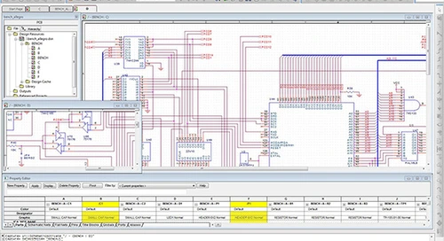
PCB schematic tools are software environments dedicated to creating detailed electrical diagrams of circuits. They use standardized symbols for components like resistors, capacitors, and integrated circuits, along with nets to represent interconnections. In PCB prototyping, these tools translate abstract ideas into verifiable blueprints, allowing engineers to simulate behavior and identify issues early. Their importance stems from enabling rapid prototyping, where time-to-market pressures demand quick validation without committing to costly hardware builds. Circuit design tools like these integrate hierarchical blocks for complex systems, supporting modularity and reuse across projects. Without them, electronics prototyping would rely on manual sketching, prone to oversights and revisions that delay progress.
The relevance in modern engineering workflows cannot be overstated. Schematic tools facilitate collaboration among design teams by providing a common language for circuit intent. They enforce design rules during entry, such as pin assignments and power distribution, aligning with industry expectations for reliability. In rapid prototyping scenarios, they cut down on trial-and-error by generating netlists directly usable in layout software. This efficiency proves vital for iterative development in fields like consumer electronics and IoT devices. Ultimately, schematic tools empower engineers to focus on innovation rather than basic documentation errors.
Core Principles of Schematic Design in PCB Prototyping
At the heart of schematic tools lies symbol libraries, which standardize representations per IPC-2221 guidelines for printed board design. Engineers select symbols with predefined footprints, electrical parameters, and datasheets, ensuring consistency from schematic to board layout. Nets automatically route signals, with bus structures grouping multi-bit lines for clarity in dense designs. Annotation features assign reference designators and values systematically, preventing duplicates and aiding bill-of-materials generation. These principles support PCB prototyping by creating error-free inputs for downstream processes like autorouting and simulation.
Hierarchical schematics further enhance manageability in complex circuits. Top-level sheets link to sub-sheets, encapsulating subsystems like power supplies or microcontrollers. This modularity aids rapid prototyping, as changes propagate efficiently without redrawing entire diagrams. Forward and back annotation synchronizes updates between schematic and layout, maintaining integrity. Engineers must verify netlist integrity using built-in checks for opens, shorts, and unconnected pins. Adhering to these mechanisms ensures designs transition smoothly to fabrication, embodying disciplined engineering practice.
Simulation integration represents another key principle. Many schematic tools embed SPICE-like engines to model analog, digital, and mixed-signal behaviors pre-layout. Timing analysis, power budgeting, and signal integrity checks occur virtually, flagging issues like excessive voltage drops. This predictive capability accelerates electronics prototyping by validating functionality without prototypes. Engineers iterate parameters directly in the schematic, observing real-time waveforms. Such principles underscore why schematic tools are indispensable for reliable PCB prototyping.
Integrating Schematic Tools with Layout and Simulation for Rapid Prototyping
Seamless integration with PCB layout software forms the backbone of efficient workflows. Schematic tools export netlists, BOMs, and component positions, populating layout canvases instantly. Design rule checks (DRC) at this junction verify spacing, trace widths, and via sizes against fabrication constraints. Rapid prototyping thrives here, as discrepancies caught early avoid respins. Engineers use cross-probing to navigate between schematic pins and layout pads, streamlining debugging. This synergy transforms circuit design tools into comprehensive platforms for end-to-end development.
Simulation bridges schematic and physical realms effectively. Pre-layout runs confirm DC operating points, AC responses, and transient behaviors using embedded models. Post-layout extraction incorporates parasitics like inductance and capacitance for accuracy. In PCB prototyping, this step predicts electromagnetic interference and thermal hotspots virtually. Tools often support Monte Carlo analysis for tolerance variations, enhancing robustness. Electric engineers leverage these features to de-risk prototypes, achieving first-pass success more frequently.
Advanced features like design reuse libraries amplify integration benefits. Pre-verified schematic blocks for common functions, such as ADCs or voltage regulators, speed up new projects. Version control systems track changes, enabling rollback if simulations reveal regressions. Collaborative environments allow multi-user edits with conflict resolution. These integrations make schematic tools central to rapid prototyping pipelines, fostering agility in competitive markets.
Best Practices for Using Schematic Tools in Electronics Prototyping
Start with thorough planning by defining requirements like voltage levels, current demands, and environmental factors upfront. Populate schematics with accurate models from verified libraries, avoiding generic placeholders. Implement power and ground planes early via net classes, ensuring low-impedance distribution per J-STD-020 sensitivity classifications. Annotate comprehensively, including tolerances and derating factors for reliability. Regular ERC (electrical rule check) runs during design catch anomalies like floating inputs. These practices minimize errors in PCB prototyping, promoting manufacturable outcomes.
Leverage hierarchy judiciously to balance detail and overview. Limit sheet count to maintain navigability, using ports for inter-sheet connections. Simulate iteratively at milestones, refining components based on results. Generate reports for design reviews, covering connectivity and BOM completeness. For rapid prototyping, automate netlist exports and use scripting for repetitive tasks. Electric engineers who follow these steps reduce prototyping cycles significantly.
Collaboration demands standardized naming conventions and shared libraries. Implement design reviews with checklists aligned to IPC standards. Version schematics with semantic numbering for traceability. Backup projects in cloud repositories for redundancy. Post-prototype, archive designs with lessons learned for future reuse. These best practices elevate schematic tools from drafting aids to strategic assets in electronics prototyping.
Case Study: Optimizing a Mixed-Signal Prototype with Schematic Tools
Consider a typical mixed-signal design for an IoT sensor node, involving an MCU, analog front-end, and power management. The engineering team began with a flat schematic, quickly overwhelming the canvas with 200 components. Switching to hierarchical blocks isolated the ADC chain and RF section, clarifying interactions. Simulation revealed noise coupling on analog lines, prompting filter additions and ground partitioning. Netlist transfer to layout triggered DRC violations on high-speed traces, resolved via back-annotation.
Rapid iterations followed: power analysis showed marginal margins under load, leading to capacitor upsizing. ERC confirmed no un-driven outputs post-changes. The prototype fabricated in days, passing functional tests on first build. Without schematic tools' integration, debugging would have extended weeks. This case illustrates how circuit design tools enable precise control in PCB prototyping, yielding reliable hardware efficiently.
Conclusion
PCB schematic tools stand as the linchpin in bridging conceptual circuits to tangible prototypes. Their structured approach to symbol management, hierarchy, and simulation integration underpins rapid prototyping success. Electric engineers benefit from reduced errors, faster iterations, and manufacturable designs adhering to key standards. By embracing best practices like iterative verification and collaboration, teams realize ideas swiftly and reliably. In electronics prototyping, these circuit design tools not only accelerate timelines but also elevate design quality. Mastering them propels projects from idea to reality with confidence.
FAQs
Q1: What role do schematic tools play in PCB prototyping?
A1: Schematic tools capture circuit intent through symbols and nets, generating netlists for layout and simulation. They enable early error detection via ERC and SPICE analysis, crucial for rapid prototyping. Engineers verify functionality pre-fabrication, aligning designs with standards like IPC-2221. This reduces respin costs and timelines in electronics prototyping workflows.
Q2: How do schematic tools support rapid prototyping?
A2: By integrating hierarchy, simulation, and netlist export, schematic tools streamline from design to board spin. Iterative checks catch issues like power imbalances early, minimizing physical builds. Cross-probing with layout aids debugging, while BOM automation speeds procurement. In PCB prototyping, this flow cuts weeks from development, ideal for time-sensitive projects.
Q3: Why are circuit design tools essential for electric engineers in electronics prototyping?
A3: Circuit design tools provide logical frameworks for complex schematics, enforcing consistency via libraries and rules. They support mixed-signal analysis and design reuse, preventing oversights in dense boards. Forward annotation ensures layout fidelity, per J-STD-020 guidelines. Engineers gain productivity, focusing on innovation over manual fixes in prototyping phases.
Q4: What best practices improve schematic efficiency in PCB prototyping?
A4: Adopt hierarchy for modularity, run ERC and simulations routinely, and use net classes for critical signals. Standardize libraries and annotate fully for reviews. Version control tracks changes, aiding collaboration. These steps enhance accuracy and speed in rapid prototyping, yielding robust prototypes aligned with industry standards.
References
IPC-2221B — Generic Standard on Printed Board Design. IPC, 2012
J-STD-020E — Moisture/Reflow Sensitivity Classification of Nonhermetic Surface Mount Devices. JEDEC, 2014
IPC-7351B — Generic Requirements for Surface Mount Design and Land Pattern Standard. IPC, 2010


