Introduction
Multi-layer printed circuit boards form the backbone of modern electronics, where signal integrity and electromagnetic interference control demand precise grounding strategies. Ground plane via stitching stands out as a critical technique to interconnect ground planes across multiple layers, ensuring a unified reference potential throughout the board. This approach directly tackles common hurdles in multilayer PCB grounding, such as impedance discontinuities and unintended potential differences. Engineers often encounter performance degradation from poor grounding, including noise coupling and radiated emissions that fail compliance tests. By implementing ground plane via stitching thoughtfully, designers can maintain stable return paths for currents, enhancing overall system reliability. This article delves into the engineering principles, practical implementation, and resolution of related issues, providing structured guidance for electric engineers working on complex PCB layouts.
What Is Ground Plane Stitching and Why It Matters
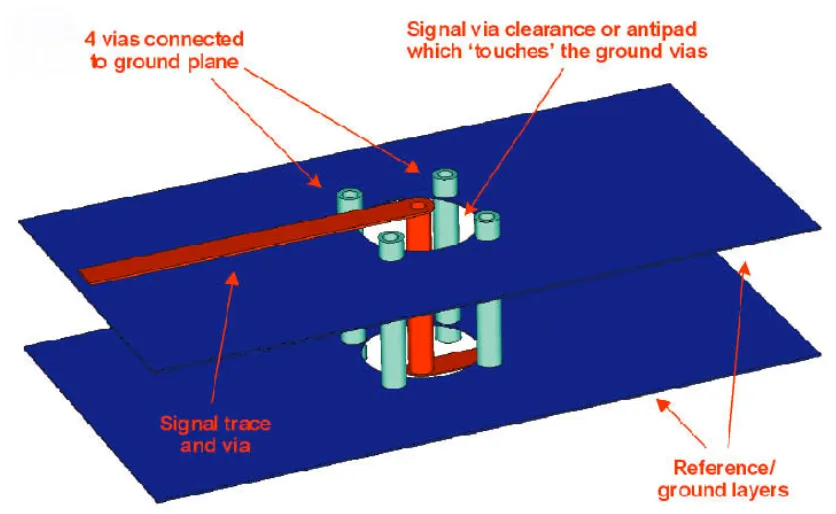
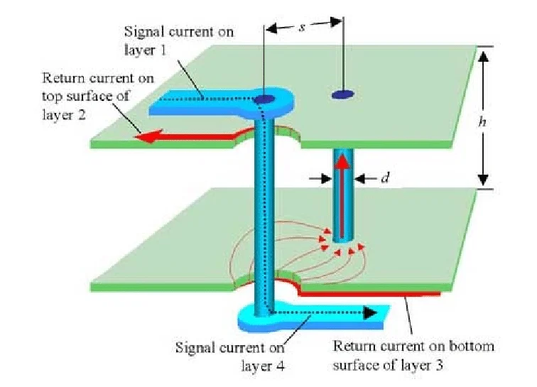
Ground plane via stitching involves placing multiple plated through-hole vias strategically to electrically connect ground planes on different layers of a multi-layer PCB. These vias act as low-inductance bridges, creating a continuous ground structure that mimics a single solid plane despite physical layer separations. In essence, stitching prevents isolated ground regions that could lead to voltage gradients under dynamic load conditions. The relevance intensifies in high-speed designs, where return currents seek the path of least impedance, potentially detouring through unintended routes if planes are not interconnected. Without stitching, multilayer PCB grounding suffers from elevated loop areas, amplifying susceptibility to crosstalk and external interference. Ultimately, this technique upholds the integrity of analog and digital signals, aligning with the demands of dense, high-performance circuits.
The matter gains urgency as board complexity rises, with layer counts exceeding eight becoming commonplace in RF and power applications. Stitching mitigates risks associated with thermal expansion, which can stress unconnected planes during fabrication and operation. It also supports consistent thermal dissipation by distributing heat across grounded copper areas. For electric engineers, mastering ground plane via stitching translates to fewer design iterations and robust prototypes that pass EMI scans on the first try. Industry practices emphasize its role in achieving predictable electrical behavior across the stackup.
Technical Principles of Ground Plane Stitching
At its core, ground plane via stitching leverages the principle of minimizing loop inductance in return current paths. In a multi-layer PCB, signals propagate between layers via transitions, and their return currents mirror these paths on adjacent ground planes. Disconnected planes force currents to travel longer routes, increasing inductance and radiated emissions according to basic electromagnetic theory. Stitching vias, spaced appropriately, provide parallel low-impedance paths that approximate an ideal infinite ground plane. This reduces voltage drops and phase shifts that could distort waveforms, particularly at frequencies where skin effect confines currents to plane surfaces.
Consider the physics of ground loops: potential differences arise when separate ground regions carry unbalanced currents, inducing noise via mutual inductance. Via stitching for ground loops shorts these regions, equalizing potentials and collapsing loop areas to negligible sizes. The effectiveness depends on via density and placement relative to signal traces, ensuring return paths stay proximate as per image plane theory. In high-frequency regimes, stitching also suppresses cavity resonances between planes by damping modal currents. IPC-2221C outlines generic requirements for plane integrity and conductor spacing, underscoring the need for continuous ground references in design.
Furthermore, stitching influences power distribution network impedance, where ground and power planes form a transmission line pair. Vias must handle peak currents without excessive heating, relying on adequate plating thickness for DC conduction. Simulations reveal that insufficient stitching elevates PDN impedance peaks, leading to voltage ripple in sensitive circuits. By distributing vias evenly, engineers achieve broadband low-impedance grounding, vital for mixed-signal boards.
Best Practices for Ground Plane Via Stitching in Multi-Layer PCBs
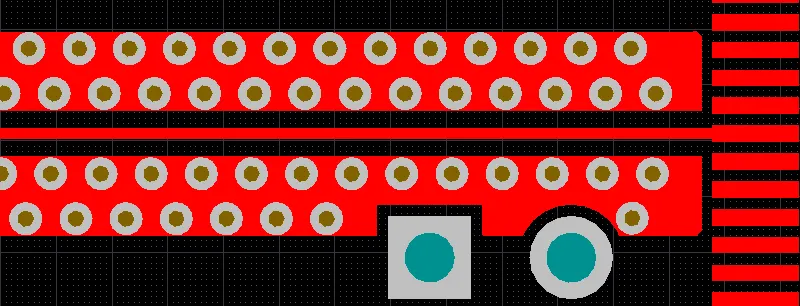
Engineers should begin by mapping signal traces to identify critical return path segments requiring stitching support. Place vias along trace transitions and around high-current components to shadow signals closely. Maintain uniform spacing across planes, prioritizing edges and splits where discontinuities loom largest. Avoid clustering vias unnecessarily, as this wastes real estate without proportional impedance gains. Integrate stitching during initial layout to prevent late-stage rerouting conflicts.
For multilayer PCB grounding, select via types suited to layer count: through-hole vias suit most cases, while blind or buried vias minimize stubs in dense designs. Ensure via diameters support fabrication tolerances, balancing drill size with annular ring integrity. Connect vias to all ground layers via net assignment, verifying continuity in design rule checks. IPC-6012F specifies performance qualifications for rigid boards, including interlayer connections that stitching must satisfy.
Address power-ground coupling by stitching both planes similarly, forming a stripline-like environment for signals. In RF sections, align stitching with guard traces to contain fields. During stackup planning, position ground planes adjacent to signal layers for optimal coupling. Post-layout, perform impedance scans to validate stitching efficacy before fabrication.
Thermal management benefits from stitching, as vias channel heat to inner planes acting as sinks. Monitor via current capacity using conservative derating for plating. Collaborate with fabricators early on aspect ratios to avoid plating voids.
Troubleshooting Grounding Issues with Via Stitching
Ground loops manifest as hum or beat frequencies in audio circuits, often traced to unstitched plane segments carrying return currents separately. Measure differential voltages across suspected regions with a scope under load to confirm. Add targeted stitching vias nearest the loop source, prioritizing high-impedance paths. Recheck after modifications, as new vias might introduce parasitic capacitance.
Excessive EMI points to sparse stitching allowing plane resonances; sweep spectrum analyzer data reveals peaks tied to board dimensions. Increase via density in resonant zones while preserving signal clearance. IPC-A-600M provides acceptability criteria for bare boards, including plane continuity that stitching enforces.
Impedance bumps from via stubs degrade eye diagrams in high-speed links. Transition to shorter vias or back-drilling if feasible. Simulate PDN before committing to layout changes.
Power plane droop under transient loads signals inadequate stitching; probe ripple and correlate with via placement. Distribute additional vias near decoupling caps for local reinforcement.
Conclusion
Ground plane via stitching proves indispensable for multilayer PCB grounding, delivering low-impedance unity across layers. By adhering to structured principles and best practices, engineers avert ground loops and EMI pitfalls effectively. Proactive troubleshooting ensures designs meet performance thresholds reliably. Integrating these techniques yields robust, compliant boards ready for demanding applications.
FAQs
Q1: What is ground plane via stitching and its role in multi-layer PCBs?
A1: Ground plane via stitching uses multiple vias to interconnect ground planes on different layers, forming a continuous low-impedance reference. This technique is essential in multi-layer PCBs to prevent isolated potentials that disrupt signal return paths. It supports high-speed operation by minimizing inductance and loop areas logically. Engineers apply it systematically during layout to enhance overall grounding integrity.
Q2: How does via stitching for ground loops improve PCB performance?
A2: Via stitching for ground loops connects disparate ground regions, eliminating voltage differentials that induce noise. In practice, it shortens return paths, reducing mutual coupling between circuits. This leads to cleaner signals and lower EMI emissions in multi-layer designs. Logical placement near sensitive traces maximizes benefits without excess vias. Troubleshooting confirms resolution through potential measurements.
Q3: What factors determine optimal spacing for ground plane via stitching?
A3: Optimal spacing for ground plane via stitching depends on signal frequencies, board size, and impedance targets. Engineers consider wavelength fractions to suppress resonances while respecting fabrication limits. Uniform grids work well for broad coverage in multilayer PCB grounding. Simulations guide refinements for specific PDN profiles. Adherence to design rules ensures manufacturability.
Q4: When should electric engineers prioritize via stitching in PCB design?
A4: Prioritize via stitching in high-speed, mixed-signal, or power-heavy multi-layer PCBs where grounding discontinuities risk integrity. It shines in layouts with plane splits or layer transitions. Early integration avoids costly respins. Per standards like IPC-2221C, it upholds plane continuity for reliable performance. Validate with post-layout analysis.
References
IPC-2221C — Generic Standard on Printed Board Design. IPC, 2023
IPC-6012F — Qualification and Performance Specification for Rigid Printed Boards. IPC, 2023
IPC-A-600M — Acceptability of Printed Boards. IPC, 2025