Introduction
High-frequency PCBs operate at frequencies typically above 500 MHz, extending into the GHz range for applications like radar systems, telecommunications, and satellite communications. These boards demand precise design to maintain signal quality and ensure long-term reliability under demanding conditions. Engineers face challenges such as signal degradation, electromagnetic interference, and material instability that can compromise performance. This article explores critical high-frequency PCB layout strategies, signal integrity in RF PCBs, controlled impedance for RF signals, RF PCB material selection, and techniques for minimizing losses in high-frequency PCBs. By addressing these factors, designers can achieve robust, high-reliability outcomes aligned with industry best practices.
Understanding High-Frequency PCBs and Their Importance
High-frequency PCBs transmit signals where wavelength approaches or becomes smaller than board dimensions, leading to transmission line effects rather than lumped circuit behavior. At these frequencies, conventional FR-4 materials often fail due to high dielectric losses and inconsistent impedance, necessitating specialized approaches. Signal integrity in RF PCBs becomes paramount as even minor discontinuities cause reflections, attenuations, or crosstalk that degrade data rates and system efficiency. Reliability is equally critical in aerospace, defense, and 5G infrastructure, where failures can have severe consequences. Proper design mitigates these risks, ensuring consistent performance over the board's lifecycle.
Key Technical Principles in High-Frequency Design
In high-frequency environments, signals propagate as electromagnetic waves along traces, governed by Maxwell's equations and characterized by characteristic impedance. The skin effect confines current to the conductor surface, increasing effective resistance and generating heat, while proximity effect further elevates losses between adjacent traces. Dielectric losses arise from the material's dissipation factor, converting signal energy into heat, especially pronounced at GHz frequencies. These mechanisms underscore the need for controlled impedance for RF signals to prevent mismatches that reflect power back to the source. Understanding these principles guides effective high-frequency PCB layout.
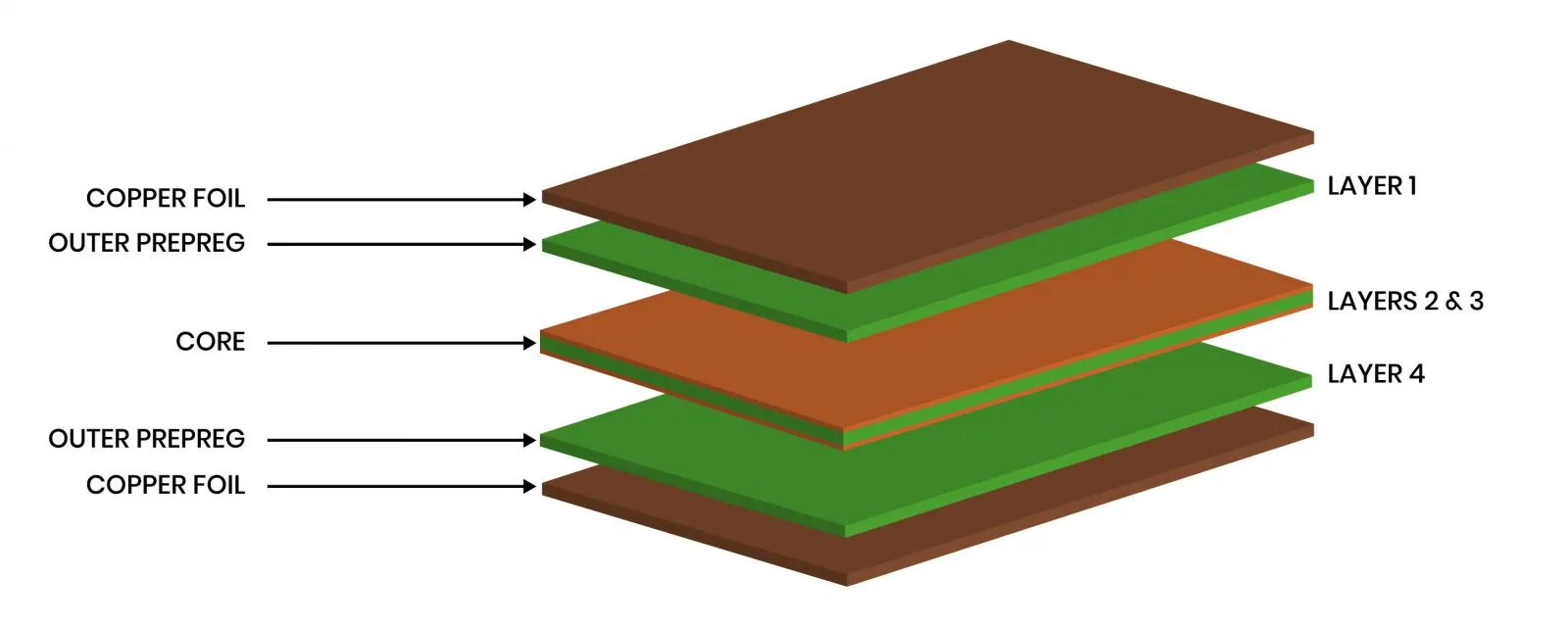
RF PCB Material Selection
RF PCB material selection focuses on low dielectric constant (Dk) for faster signal speeds and low dissipation factor (Df) to minimize losses in high-frequency PCBs. Materials must exhibit stability across temperature, humidity, and frequency variations to maintain controlled impedance for RF signals. Hybrid stackups combining low-loss cores with cost-effective outer layers balance performance and manufacturability. Engineers evaluate tan δ values and coefficient of thermal expansion (CTE) to ensure mechanical reliability. Adherence to IPC-6018 qualification standards verifies material suitability for microwave applications through electrical and environmental testing.
Glass transition temperature and moisture absorption influence long-term reliability, as absorbed water increases Dk and Df, exacerbating signal integrity in RF PCBs. Designers prioritize materials with consistent properties to avoid warpage or delamination during thermal cycling.
Achieving Controlled Impedance for RF Signals
Controlled impedance for RF signals requires precise control of trace width, thickness, dielectric height, and Dk in microstrip or stripline configurations. Simulations predict impedance using field solvers, accounting for manufacturing tolerances like etch variation and plating thickness. Reference planes provide return paths, minimizing radiation and loop inductance. Symmetry in differential pairs preserves balance and common-mode rejection. High-frequency PCB layout must incorporate these elements to match source and load impedances, typically 50 ohms single-ended or 100 ohms differential.
Fabrication processes demand tight tolerances, often ±10% for impedance, verified post-production with time-domain reflectometry. Ground via stitching around traces reduces slotline modes and enhances shielding.
Signal Integrity in RF PCBs
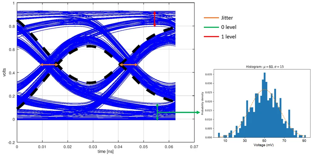
Signal integrity in RF PCBs hinges on minimizing reflections from impedance discontinuities, such as bends, vias, or pads. Eye diagrams reveal jitter, attenuation, and crosstalk impacts, guiding iterative design refinements. Crosstalk arises from capacitive and inductive coupling, mitigated by 3W spacing rules between traces and solid ground planes. Vias introduce stubs and inductance; blind, buried, or back-drilled types preserve integrity. Proper termination absorbs reflections, while equalization compensates for losses.
Power integrity complements signal concerns, as voltage droops from plane splits or decoupling inadequacies couple noise onto signals. Comprehensive modeling integrates these factors for holistic optimization.
High-Frequency PCB Layout Best Practices
High-frequency PCB layout prioritizes short, straight traces with minimal vias to reduce parasitic effects. Routed signals follow curved paths with 45-degree bends or smooth arcs to avoid reflections from sharp corners. Dedicated ground planes on adjacent layers form striplines, confining fields and suppressing radiation. Component placement groups RF sections away from digital noise sources, with shielding cans or moats for isolation. Symmetry in length-matched pairs prevents skew in differential signaling.
Thermal management integrates vias under power components and wide pours for heat spreading, preventing hotspots that degrade materials. IPC-2228 provides guidelines for RF board design, emphasizing layout for performance and manufacturability.
Minimizing Losses in High-Frequency PCBs
Minimizing losses in high-frequency PCBs targets conductor, dielectric, and radiation components. Wider traces or thicker copper reduce skin effect losses, balanced against impedance requirements. Low-profile copper foils lower surface roughness, decreasing insertion loss at GHz frequencies. Dielectric selection with Df below 0.005 preserves signal amplitude over distance. Enclosed striplines outperform exposed microstrips by reducing radiation and external coupling.
Radiation losses stem from unbalanced fields; symmetric stackups and via fences contain emissions. Environmental testing per IPC-6018 confirms low-loss performance under vibration and temperature extremes.
Ensuring High-Reliability Through Qualification
High-reliability demands rigorous qualification, including thermal shock, humidity bias, and high-frequency electrical testing. Solderability preservation prevents assembly defects, while CTE matching avoids via cracking. Mechanical robustness counters flexure in conformal coated boards. Lifecycle predictions use acceleration factors from standards testing.
Conclusion
High-frequency PCB design for reliability integrates RF PCB material selection, controlled impedance for RF signals, and meticulous high-frequency PCB layout to uphold signal integrity in RF PCBs. Minimizing losses in high-frequency PCBs through principled choices yields efficient, durable boards. Engineers applying these strategies, informed by IPC standards, deliver superior performance in critical applications. Continuous simulation and verification bridge design to fabrication, ensuring success.
FAQs
Q1: What factors drive RF PCB material selection for high-reliability applications?
A1: RF PCB material selection prioritizes low Dk and Df for minimal losses, along with thermal stability and low moisture absorption. Materials must support controlled impedance for RF signals across operating temperatures. Mechanical properties like CTE matching prevent stress failures. Testing per IPC standards verifies suitability, balancing cost and performance for long-term signal integrity in RF PCBs.
Q2: How does high-frequency PCB layout impact signal integrity in RF PCBs?
A2: High-frequency PCB layout affects signal integrity in RF PCBs by controlling trace geometry, via usage, and plane integrity to minimize reflections and crosstalk. Straight routing, proper spacing, and ground stitching reduce losses. Simulations optimize for eye opening and jitter. Adhering to layout rules ensures reliable propagation at GHz frequencies.
Q3: Why is controlled impedance for RF signals essential in high-frequency designs?
A3: Controlled impedance for RF signals prevents mismatches causing reflections and power loss in high-frequency PCBs. Precise stackup and trace dimensions maintain 50-ohm characteristics. Tolerances account for fab variations. This foundation supports signal integrity in RF PCBs, enabling high data rates without degradation. Verification post-fab confirms compliance.
Q4: What techniques minimize losses in high-frequency PCBs?
A4: Minimizing losses in high-frequency PCBs involves low-Df materials, smooth copper foils, and enclosed transmission lines. Reducing vias and optimizing bend radii cuts conductor losses. Solid reference planes suppress radiation. These practices, combined with impedance control, preserve signal strength over distance for reliable RF performance.
References
IPC-6018D — Qualification and Performance Specification for High Frequency (Microwave) Printed Boards. IPC
IPC-2228 — Sectional Design Standard for Radio Frequency Printed Boards. IPC, 2022


