Introduction
Selecting the right PCB prototyping service is critical for electrical engineers working on time-sensitive projects. A poor choice can lead to delays, increased costs, and design flaws that compromise functionality. In today's competitive electronics landscape, services offering quick turn PCB prototyping enable rapid iteration and validation. This comprehensive PCB prototyping service comparison evaluates key factors like capabilities, turnaround times, and quality assurance. By focusing on these elements, engineers can minimize risks and optimize their development workflow. Ultimately, the goal is to partner with a service that aligns with project specifications and reliability needs.
What Is PCB Prototyping and Why It Matters
PCB prototyping involves the fabrication and assembly of small quantities of printed circuit boards to test designs before full-scale production. These prototypes allow engineers to verify electrical performance, mechanical fit, and thermal behavior in real-world conditions. Quick turn PCB prototyping services accelerate this process, often delivering boards within days rather than weeks. For electrical engineers, this matters because it shortens the design cycle, reduces time-to-market, and prevents costly errors in mass production. In complex projects with high-density interconnects or mixed-signal circuits, reliable prototyping ensures compliance with performance requirements. Without effective prototyping, projects risk failure due to unaddressed issues like signal integrity or power distribution problems.
Key Factors for PCB Prototyping Service Comparison
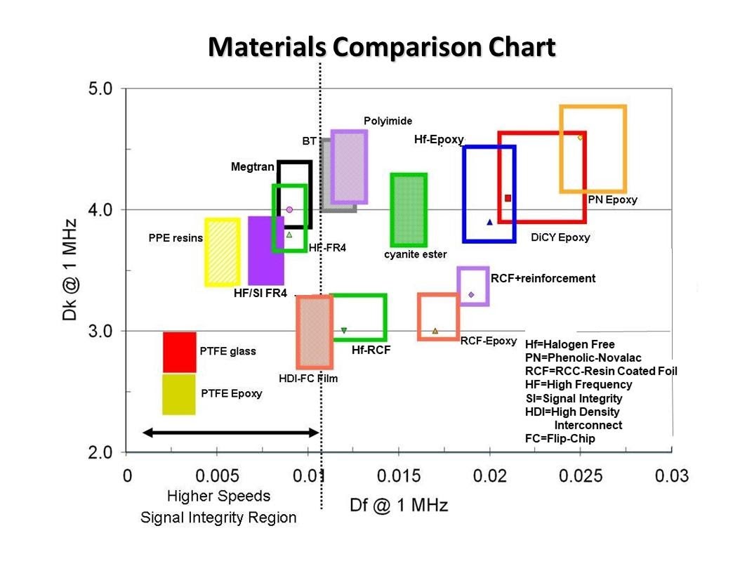
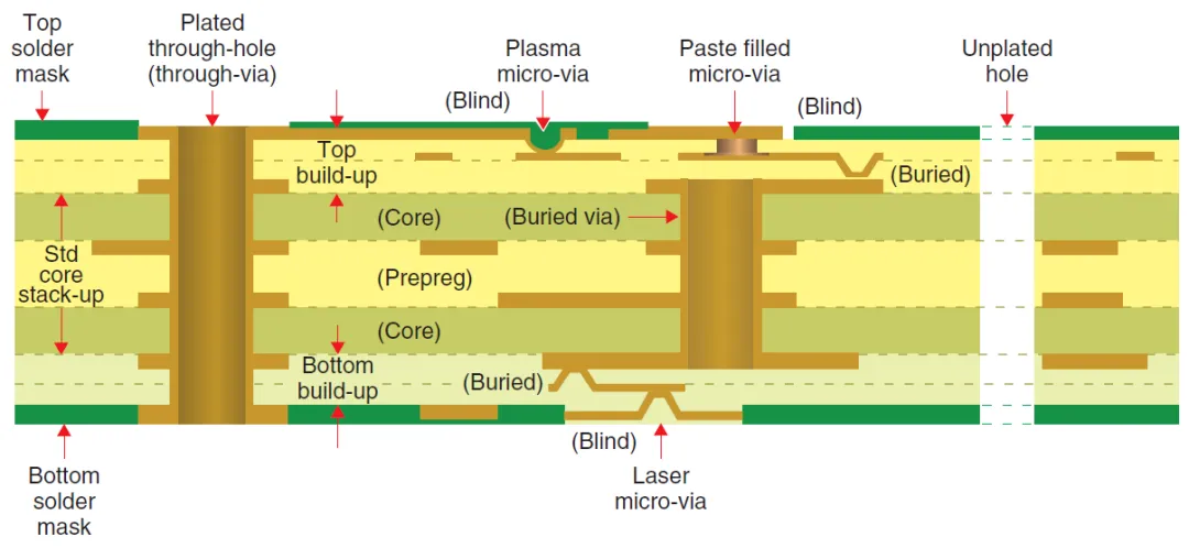
When conducting a PCB prototyping service comparison, start with the service's technical capabilities. Evaluate supported layer counts, from single-layer to multilayer boards up to 20 layers or more, and minimum trace widths typically in the 3-5 mil range for high-density designs. Board sizes, panelization options, and impedance control are also essential for RF or high-speed applications. Services should handle standard materials like FR-4 with varying thicknesses, along with advanced options for flexibility or high-temperature needs. Surface finishes such as ENIG, HASL, or OSP affect solderability and shelf life, so confirm compatibility with downstream assembly. A mismatch in capabilities can force design compromises or require multiple vendors.
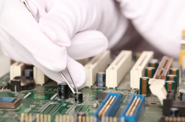
Next, assess PCB assembly services integration. Many prototyping providers offer turnkey solutions combining fabrication with surface-mount technology (SMT) and through-hole (THT) assembly. Look for support of fine-pitch components, BGA packages, and mixed-technology boards. Pick-and-place accuracy, reflow soldering profiles, and automated optical inspection (AOI) are vital for yield. Engineers benefit from services that provide functional testing or in-circuit testing to validate prototypes early. Seamless fab-to-assembly flow reduces handling risks and shipping times.
Turnaround Time and Quick Turn PCB Prototyping
Quick turn PCB prototyping distinguishes top services in fast-paced development. Standard lead times range from 5-10 days, but express options deliver in 24-48 hours for simple boards. Factors influencing speed include file complexity, queue volume, and factory automation levels. For urgent projects, confirm rush fees and availability without quality trade-offs. Delays often stem from design rule violations or material shortages, so prioritize services with instant design-for-manufacturability (DFM) feedback. This ensures files are production-ready upon upload.
PCB fabrication cost varies significantly based on these timelines. Simpler boards with fewer layers and standard drills cost less per unit, while high-layer-count or blind-via designs increase expenses. Volume discounts apply even in prototyping, so ordering panels optimizes per-board pricing. Hidden costs like shipping, tooling, or rework should be transparent in quotes. Engineers must balance speed and budget by requesting itemized breakdowns early.
Quality Control and Standards Compliance
Quality assurance is non-negotiable in PCB prototyping service comparison. Reputable services adhere to IPC-6012E for rigid printed boards, ensuring consistent plating thickness, solder mask adhesion, and bow/warp limits. Visual and electrical testing, including flying probe for opens/shorts, detects defects early. For assembly, IPC-A-600K acceptability criteria guide inspection of solder joints and component placement. Certifications like ISO 9001:2015 signal robust process controls and traceability.
Traceability from raw materials to finished boards prevents counterfeit components or contamination issues. Request documentation like certificates of conformance (CoC) and first-article inspection (FAI) reports. In high-reliability applications, such as automotive or aerospace, JEDEC J-STD-020E moisture sensitivity handling protects components during reflow. Neglecting quality leads to field failures, rework expenses, and eroded trust in the design.
Cost Analysis: Understanding PCB Fabrication Cost
PCB fabrication cost breaks down into material, processing, and overhead components. Base costs depend on board area, copper weight, and drill density, with vias and slots adding premiums. Layer transitions from 2 to 8 layers can double expenses due to lamination and alignment precision. Controlled impedance or edge plating requires additional steps like etching or plating. Assembly costs scale with component count, sourcing, and programming for specific ICs.
To compare effectively, use online PCB prototyping quote tools for apples-to-apples pricing. Factor in minimum order quantities (MOQs), often as low as 5-10 units for prototypes. Economies emerge at 50+ units, blending prototyping with pilot runs. Always verify non-recurring engineering (NRE) fees for custom stencils or fixtures. Transparent pricing builds confidence in total ownership cost.
- Layer Count: Basic 1-4 layers; Advanced 8-20+ layers
- Quick Turn Time: Basic 5-7 days; Advanced 24-72 hours
- Min Trace/Spacing: Basic 6/6 mil; Advanced 3/3 mil
- Assembly Options: Basic SMT only; Advanced SMT + THT + Testing
- Quality Standards: Basic IPC Class 2; Advanced IPC Class 3
- Typical Cost per Board: Basic lower for volume; Advanced higher for complexity
Best Practices for Selecting Online PCB Prototyping Services
Leverage online PCB prototyping platforms for instant quoting and file uploads in standard formats like Gerber RS-274X or ODB++. Instant DFM analysis flags issues like annular ring violations or drill breakout. Compare at least three services across capabilities, cost, and reviews from engineering forums. Prioritize those with engineering support for stackup advice or material selection.
Develop a checklist: Does the service support your board outline, including tabs or scoring? Confirm impedance tolerances if needed, typically ±10%. For assembly, provide bill-of-materials (BOM) and centroid files accurately. Test small orders first to gauge consistency. Track metrics like yield rate and on-time delivery for future decisions.
Troubleshooting Common Prototyping Pitfalls
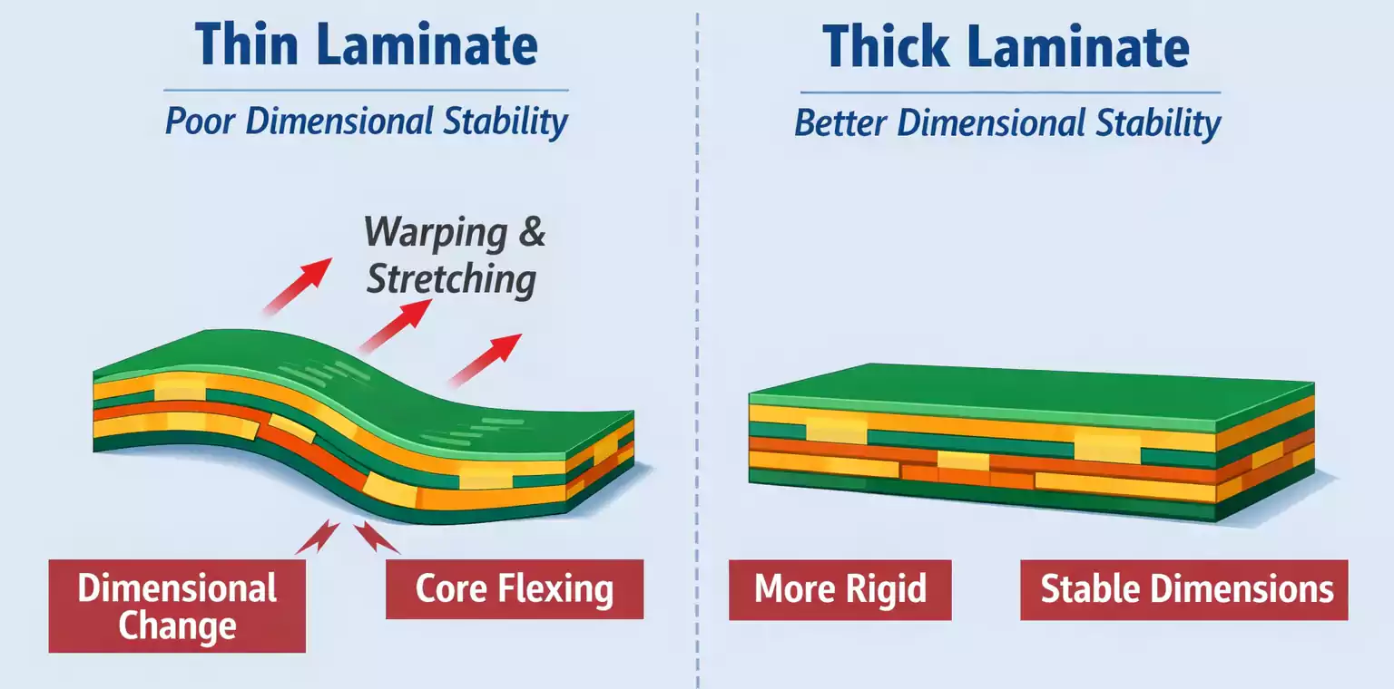
Engineers often encounter warpage in prototypes due to asymmetric copper distribution or improper baking. Mitigate by requesting stress-relief processes post-fabrication. Solder joint voids in assembly arise from flux residue or profile mismatches; opt for services using no-clean flux and profile verification. Component misalignment from stencil misalignment requires laser-cut stencils over framed ones. Always review incoming inspection photos before approving production. These steps, grounded in practical experience, enhance prototype reliability.
Conclusion
Choosing the right PCB prototyping service demands a structured PCB prototyping service comparison across capabilities, speed, cost, and quality. Prioritize quick turn PCB prototyping for agility, while ensuring PCB assembly services meet project needs. Adherence to standards like IPC-6012E guarantees performance. By following best practices and using online tools, electrical engineers streamline development and reduce risks. Invest time upfront to save significantly downstream. This approach positions projects for successful scaling to production.
FAQs
Q1: What should electrical engineers consider in a PCB prototyping service comparison?
A1: Focus on layer support, minimum feature sizes, and quick turn PCB prototyping options to match design complexity. Evaluate PCB assembly services for integrated SMT and testing capabilities. Check quality via IPC standards compliance and DFM feedback. Transparent PCB fabrication cost breakdowns prevent surprises. This ensures prototypes validate designs efficiently without delays.
Q2: How does PCB fabrication cost impact quick turn PCB prototyping choices?
A2: PCB fabrication cost rises with layer count, via density, and rush premiums in quick turn scenarios. Balance by panelizing boards and selecting standard materials. Online PCB prototyping quotes reveal trade-offs instantly. Prioritize services offering volume discounts even for prototypes. Accurate BOMs minimize assembly surcharges.
Q3: Why integrate PCB assembly services in prototyping?
A3: Combining PCB assembly services with fabrication reduces handling risks and accelerates testing. It enables functional validation of soldered boards early. Look for AOI and X-ray inspection to catch defects. This streamlines iteration for electrical engineers.
Q4: What role do standards play in online PCB prototyping?
A4: Standards like IPC-A-600K ensure consistent quality in online PCB prototyping outputs. They guide inspection criteria for solder masks and plating. Compliance verifies prototypes suit production transition. Request CoCs for traceability.
References
IPC-6012E — Qualification and Performance Specification for Rigid Printed Boards. IPC, 2017
IPC-A-600K — Acceptability of Printed Boards. IPC, 2020
JEDEC J-STD-020E — Moisture/Reflow Sensitivity Classification. JEDEC, 2014
ISO 9001:2015 — Quality Management Systems. ISO, 2015