Introduction
In high-speed PCB designs, maintaining precise timing is crucial for reliable operation. Jitter introduces unwanted variations in signal edges, compromising PCB signal integrity and leading to data errors or system failures. Electrical engineers face increasing challenges as clock frequencies rise and data rates climb into gigabits per second. This guide explores jitter sources in PCB, clock jitter measurement techniques, and proven strategies for PCB jitter reduction. By understanding these elements, designers can achieve jitter-free PCBs through thoughtful layout and design choices. The focus here is on practical steps that align with engineering principles to ensure robust performance.
What Is Jitter and Why It Matters in PCB Design
Jitter refers to the deviation of a signal's edges from their ideal positions in time, particularly evident in clock signals. This timing uncertainty accumulates across the PCB, degrading signal integrity and reducing eye openings in high-speed links. In digital systems, excessive jitter causes setup and hold violations, bit errors, and synchronization failures. For electrical engineers working on multi-gigabit interfaces, controlling jitter is essential to meet timing budgets and prevent intermittent issues. Poor jitter management not only affects data throughput but also increases power consumption due to retransmissions. Ultimately, jitter-free designs enhance overall system reliability and compliance with performance specifications.
Jitter manifests in various forms, each with distinct characteristics. Random jitter arises from thermal noise and follows a Gaussian distribution, making it unbounded but predictable statistically. Deterministic jitter stems from systematic issues like reflections or crosstalk, appearing as bounded peaks in histograms. Total jitter combines these, directly impacting bit error rates in serial links. Engineers must quantify both to predict system margins accurately. Addressing jitter early in the design phase prevents costly respins and ensures scalability for future upgrades.
Jitter Sources in PCB: Identifying Common Culprits
Several factors within the PCB contribute to jitter sources in PCB, starting with power supply variations. Fluctuations from ripple, inadequate regulation, or noise coupling into rails cause timing shifts in clock drivers. Overloaded voltage regulators exacerbate this, introducing deterministic components tied to load changes. Engineers should prioritize stable power delivery to minimize these effects from the outset.
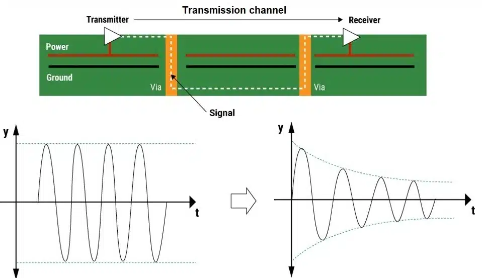
Switching noise, or simultaneous switching noise, generates ground bounce and voltage droops when multiple outputs toggle together. This data-dependent jitter peaks during high-activity periods, distorting clock edges. In dense high-speed boards, transistor switching currents couple aggressively into adjacent traces. Proper current distribution via planes helps mitigate this source.
Power distribution network impedance discontinuities lead to PDN noise, where voltage spikes modulate signals. High-frequency resonances in decoupling schemes amplify random jitter. Crosstalk from electromagnetic coupling between parallel traces shifts phases, adding periodic jitter. Reflections from unmatched impedances or stubs cause ringing, delaying edge arrivals and compounding timing errors.
Dielectric materials with high loss tangents act as low-pass filters, attenuating harmonics and increasing jitter at higher frequencies. Non-uniform trace geometries create impedance mismatches, fostering further reflections. External interference, like EMI from nearby circuits, injects additional noise. Identifying these jitter sources in PCB through simulation allows targeted fixes during layout.
Clock Jitter Measurement: Essential Techniques for Engineers
Accurate clock jitter measurement is foundational for verifying PCB signal integrity. Time-domain methods include period jitter, which compares each cycle to the ideal average over thousands of periods. Per JEDEC JESD65B standards, engineers assess signals across 10,000 clock cycles for statistically valid period jitter data. Cycle-to-cycle jitter captures delta between adjacent periods, highlighting short-term variations. Time interval error measures edge deviations from an ideal reference.
Eye diagrams provide a comprehensive view by overlaying multiple signal acquisitions. A narrow eye width signals excessive jitter, while height indicates noise margins. Engineers analyze crossing percentages and rise times to quantify distortions. Mask testing automates failure detection against predefined limits. Oscilloscope bandwidth must exceed the signal's fundamental by at least three times for fidelity.
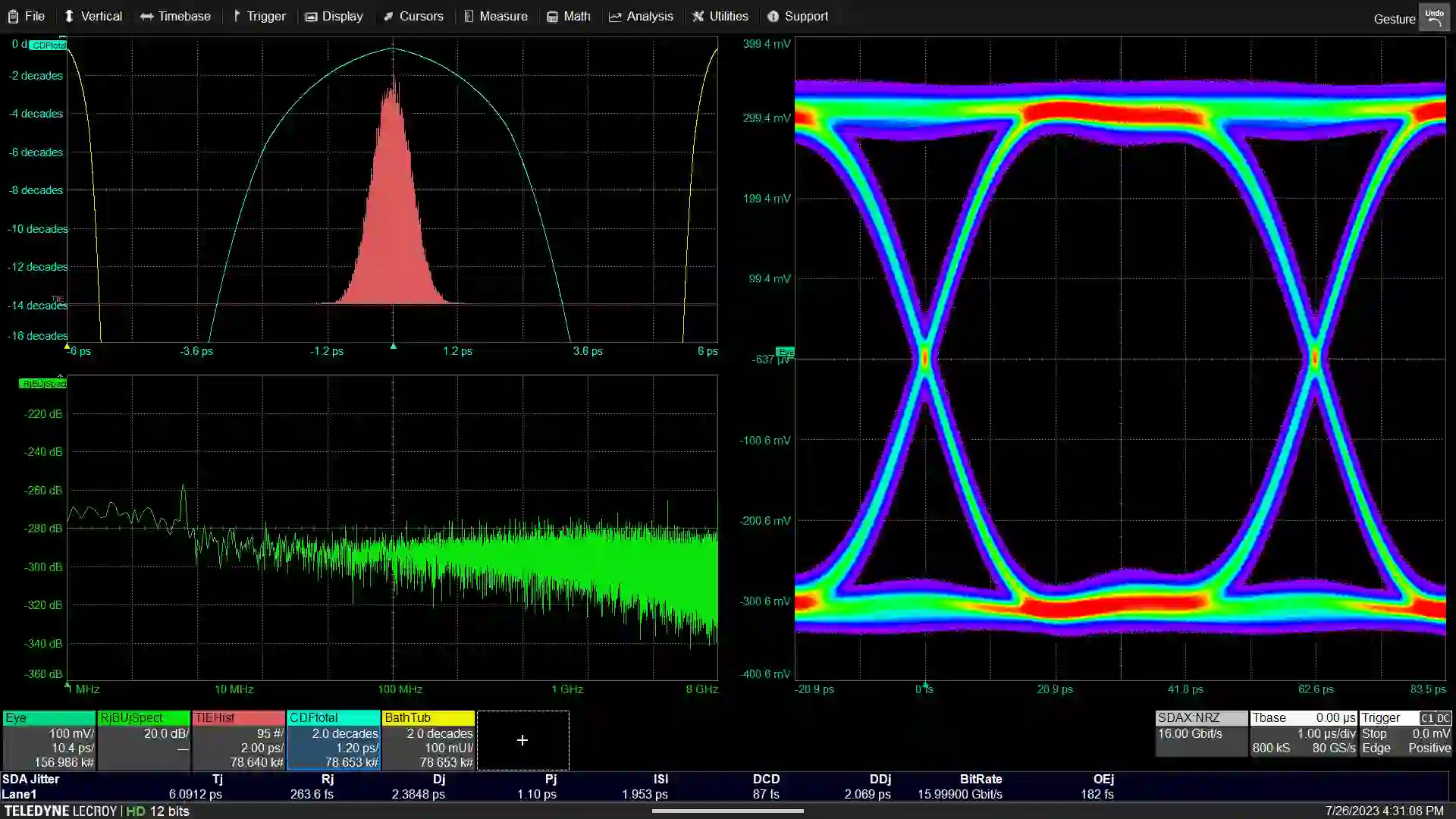
Frequency-domain analysis via phase noise spectra reveals jitter contributions at specific offsets. Integrating phase noise yields RMS jitter values for random components. Combining these methods ensures thorough characterization. Post-layout simulations correlate measurements to design choices, guiding iterations.
Practical Solutions for Reducing Jitter in PCBs
Reducing jitter in PCBs demands disciplined layout practices, beginning with controlled impedance traces. Maintain consistent widths and spacing per IPC-2221 guidelines for routing and conductor sizing to minimize variations. Use stackups with symmetric layers to avoid warpage-induced mismatches. Differential pairs offer inherent noise rejection for clocks.
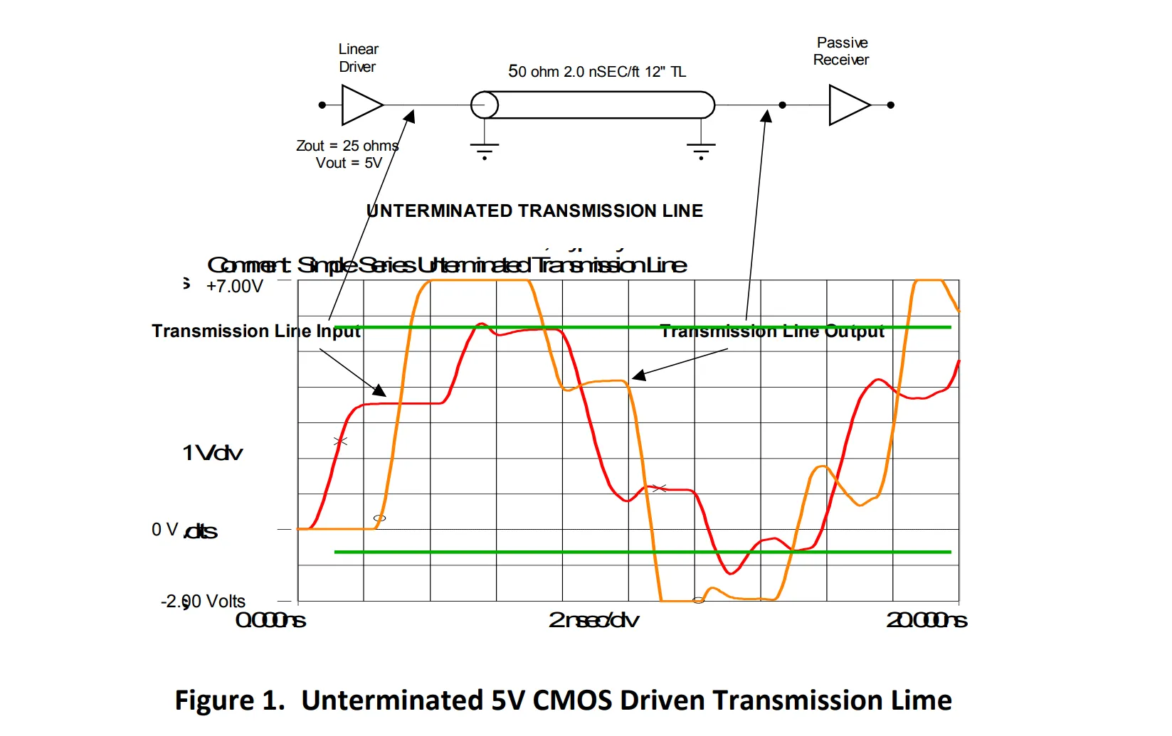
Proper termination prevents reflections, a major jitter contributor. Series termination at the driver matches source impedance, while parallel or Thevenin schemes absorb energy at receivers. AC termination suits high frequencies by bypassing DC. Place resistors as close as possible to endpoints for effectiveness.
Decoupling capacitors near clock drivers and receivers filter PDN noise effectively. Select values for target frequencies, ensuring low ESL. Solid ground and power planes provide low-impedance return paths, reducing SSN. Avoid splitting planes under high-speed signals to prevent resonance.
Route clocks away from high-current traces and analog sections to curb crosstalk. Length-match critical nets to eliminate skew. Employ low-loss dielectrics for minimal attenuation. Clock buffers with low output impedance clean up jitter propagation. These steps collectively enable PCB jitter reduction without exotic materials.
Troubleshooting Jitter Issues in High-Speed Designs
Engineers often encounter persistent jitter despite best efforts. Start by reviewing PDN integrity, simulating impedance profiles below 1 ohm up to Nyquist. Excessive via count or stub lengths signal routing flaws. Eye diagram closure at specific patterns points to data-dependent jitter from ISI.
Power supply ripple exceeding 1% of Vdd typically correlates with elevated random jitter. Inject noise to isolate contributions. Ground bounce manifests in cycle-to-cycle peaks; add stitching vias liberally. If phase noise dominates, scrutinize oscillator quality and shielding.
Iterative measurement post-prototype refines designs. Correlate simulations to hardware discrepancies for process tweaks. Consistent application yields jitter budgets under 10% of UI.
Conclusion
Achieving jitter-free PCBs hinges on addressing jitter sources in PCB through precise layout and verification. Key practices like impedance control, termination, and PDN optimization directly enhance PCB signal integrity. Clock jitter measurement via eye diagrams and standards like JEDEC JESD65B provides quantifiable feedback. Electrical engineers benefit from integrating these from schematic to fabrication. Robust designs withstand real-world stresses, ensuring long-term reliability. Prioritize these principles for superior high-speed performance.
FAQs
Q1: What are the main jitter sources in PCB designs?
A1: Jitter sources in PCB include power supply noise, crosstalk, reflections from impedance mismatches, and switching noise. PDN discontinuities and high-loss dielectrics also contribute significantly. Engineers mitigate these via stable power delivery and controlled routing. Proper identification early prevents signal integrity degradation in high-speed systems.
Q2: How can engineers achieve PCB jitter reduction in layouts?
A2: PCB jitter reduction involves uniform trace impedances, proper termination schemes, and solid ground planes. Decoupling capacitors filter noise near drivers, while length matching eliminates skew. Avoid routing clocks near noisy areas. These practices, aligned with IPC-2221, ensure minimal timing variations.
Q3: What methods are used for clock jitter measurement?
A3: Clock jitter measurement relies on period jitter over 10,000 cycles per JEDEC JESD65B, cycle-to-cycle analysis, and eye diagrams. Eye width quantifies total jitter effects on margins. Oscilloscopes overlay signals for intuitive assessment. Combine time and frequency domains for complete profiles.
Q4: Why is PCB signal integrity critical for jitter control?
A4: PCB signal integrity directly counters jitter by preserving edge timing and amplitude. Reflections and noise erode margins, causing errors. Best practices like differential signaling and low-impedance planes maintain quality. Neglect leads to bit errors in gigabit links.
References
IPC-2221 — Generic Standard on Printed Board Design. IPC
JEDEC JESD65B — Definitions of Jitter. JEDEC


