Introduction
Organic substrate PCBs serve as critical interconnect platforms in advanced semiconductor packaging, supporting high pin counts and dense routing for applications like flip-chip ball grid arrays. Proper PCB layer stackup design directly influences signal integrity by controlling impedance mismatches and minimizing losses at high frequencies. Engineers must prioritize symmetric layering and precise dielectric control to prevent reflections and crosstalk in these thin, multilayer structures. This article explores PCB layer stackup strategies tailored for organic substrates, focusing on controlled impedance PCB techniques and signal integrity layer stackup optimization. By adhering to established PCB design rules, designers can achieve reliable performance in demanding environments. Understanding these principles enables electric engineers to balance electrical performance with manufacturability constraints.
Understanding Organic Substrate PCB Layer Stackup
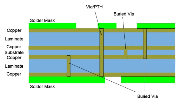
Organic substrate PCBs utilize resin-based dielectrics, such as build-up films, to create fine-line multilayer structures with layer counts often exceeding eight. The PCB layer stackup refers to the sequential arrangement of conductive layers, dielectrics, and planes, which dictates signal propagation characteristics. In these substrates, core layers provide mechanical stability while build-up layers enable microvias for high-density interconnects. Signal integrity layer stackup becomes paramount as operating frequencies push beyond gigahertz ranges, where uncontrolled impedance leads to waveform distortion. Why does this matter? Poor stackup choices amplify issues like return path discontinuities, compromising data rates in high-speed interfaces.
Effective stackups pair high-speed signal layers adjacent to reference planes, ensuring low-inductance return currents. Organic materials offer low dielectric constants around 3 to 4, aiding faster signal speeds compared to traditional FR-4. However, their thinner profiles demand meticulous planning to maintain uniformity across the panel. IPC-2221 outlines generic requirements for such organic printed board designs, emphasizing layer sequencing for integrity.
Core Technical Principles for Signal Integrity
Signal integrity in organic substrate PCBs hinges on maintaining characteristic impedance, typically 50 ohms single-ended or 100 ohms differential, through precise geometry control. The primary factors include trace width, dielectric thickness, and reference plane proximity, as governed by transmission line theory. Microstrip and stripline configurations dominate, with striplines preferred for better shielding against external noise. Crosstalk arises from capacitive and inductive coupling between adjacent traces, mitigated by increasing spacing proportional to the square root of frequency. Return path integrity relies on continuous ground or power planes directly beneath signal layers, reducing loop inductance.
Dielectric losses increase with frequency due to material tan delta, necessitating low-loss resins in outer layers. Asymmetric stackups induce warpage during thermal cycling, as differing coefficients of thermal expansion cause bowing. Engineers calculate impedance using field solvers, iterating stackup until tolerances meet ±10%. PCB design rules enforce minimum clearances to avoid field fringing at vias. These principles ensure signals propagate with minimal attenuation and phase shift.
Achieving Controlled Impedance in Organic Substrate PCBs
Organic substrate PCB impedance control requires tight tolerances on dielectric heights, often 20 to 50 microns per build-up layer. Designers specify trace widths from 20 to 50 microns for high-speed lines, adjusting for copper weight and etch factors. Reference planes must be stitched with vias every quarter wavelength to contain fields and provide low-impedance returns. Differential pairs demand symmetric spacing and length matching within 10 mils to preserve mode purity. Prepreg and resin-coated copper selection influences effective dielectric constant, critical for broadband matching.
Stackup symmetry, with mirror-imaged signal layers around the core, prevents camber during lamination. Vias introduce discontinuities, so blind and buried types minimize stub lengths in signal paths. IPC-6015 specifies qualification for organic laminate substrates, including impedance verification through time-domain reflectometry. Manufacturing variations, like resin flow, necessitate design margins of 10 to 15%. Testing coupons on panels validate stackup predictions before full production. Practical PCB design rules include ground plane splits limited to 10 mils under traces and clearance rules scaling with density. Engineers simulate eye diagrams to quantify jitter and overshoot from stackup choices.
Best Practices for Signal Integrity Layer Stackup
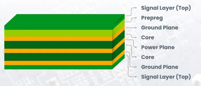
Begin with power and ground plane allocation, dedicating inner layers to broad planes for decoupling capacitance. Signal layers should sandwich between planes, following a ground-signal-power-signal-ground pattern for balanced shielding. For 10-layer organic substrates, outer layers handle low-speed signals to ease impedance control amid surface roughness. Core thickness dominates mechanical rigidity, typically 100 to 200 microns, while build-ups add fine features.
Incorporate embedded planes or thin dielectrics for planar capacitance, reducing via inductance. Avoid splitting planes under high-speed traces; instead, use moats with stitching for isolation. Thermal management integrates with stackup by placing heat-generating layers near dissipating planes. Adherence to these practices aligns with IPC-2221 guidelines for multilayer organics.
Route critical nets first, reserving adjacent layers for their references. Post-layout extraction verifies impedance profiles against targets. Collaboration with fabricators refines stackup drawings, specifying sequential build processes.
Addressing Challenges in Organic Substrate Designs
Warpage poses a major hurdle in thin organic substrates, exacerbated by CTE mismatches between copper and resin. Symmetric stackups counteract this by balancing stresses on both sides of the core. High layer counts amplify via density, risking resin squeeze-out and shorts; thus, laser drilling follows strict registration. Signal skew in length-mismatched pairs demands serpentine tuning within layer constraints.
Crosstalk in dense routing exceeds budgets without guard traces or shielding vias. Power delivery noise couples through plane resonances, mitigated by interplane capacitance. Troubleshooting involves S-parameter measurements on prototypes, correlating to stackup simulations. Iterative refinements ensure compliance.
Conclusion
Optimizing PCB layer stackup for organic substrates demands a holistic approach integrating impedance control, symmetry, and reference plane strategies. Electric engineers benefit from structured PCB design rules that prioritize signal integrity layer stackup for high-speed reliability. By applying these principles, designs achieve minimal losses and robust performance. Future trends toward finer pitches reinforce the need for precise stackups. Mastering these techniques elevates product quality and speeds time-to-market.
FAQs
Q1: What role does PCB layer stackup play in organic substrate PCB impedance control?
A1: PCB layer stackup determines organic substrate PCB impedance by defining dielectric thicknesses and reference plane distances, essential for 50-ohm matching. Symmetric arrangements minimize variations from manufacturing tolerances. Engineers use field solvers to predict profiles, ensuring signals maintain integrity up to multi-gigabit rates. Adhering to design rules prevents reflections and supports controlled impedance PCB fabrication.
Q2: How do PCB design rules enhance signal integrity layer stackup?
A2: PCB design rules specify trace spacing, via placement, and plane stitching to optimize signal integrity layer stackup. They enforce ground-signal alternation, reducing crosstalk by over 20 dB in dense organics. Minimum clearances scale with frequency, while symmetry rules combat warpage. These guidelines align stackups with fabrication capabilities for reliable high-speed performance.
Q3: Why is controlled impedance PCB critical for organic substrates?
A3: Controlled impedance PCB prevents signal distortion in organic substrates by matching trace geometry to driver loads. It relies on precise layer stackup to control fields, vital for data integrity in packaging applications. Tolerances under ±10% ensure low bit error rates. Without it, reflections degrade eye openings at high frequencies.
Q4: What are key considerations for multilayer PCB layer stackup in signal integrity?
A4: Multilayer PCB layer stackup prioritizes plane pairing for return paths and low-loss dielectrics for minimal attenuation. Symmetry avoids thermal warpage, while via optimization reduces stubs. Testing validates impedance across frequencies. These factors maximize signal integrity in organic designs per industry standards.
References
IPC-2221 — Generic Standard on Printed Board Design. IPC
IPC-6015 — Qualification and Performance Specification for Organic Laminate Multichip Module Substrates (MCM-L). IPC
IPC-6012E — Qualification and Performance Specification for Rigid Printed Boards. IPC, 2017


