Introduction
Diving into PCB design can feel overwhelming for electronic hobbyists, but starting with simple schematic tools makes the process approachable and fun. Schematics serve as the foundation of any easy PCB design project, acting like a roadmap that outlines how components connect electrically before moving to the physical board layout. For beginners, mastering these tools unlocks the ability to turn ideas into working circuits, whether it's a simple LED blinker or a sensor module. This guide focuses on beginner PCB design software features that prioritize simplicity, helping hobbyists learn PCB design without steep learning curves. By following structured steps, you’ll build confidence and avoid common pitfalls right from the start. Let’s explore how simple schematic tools empower your projects.
What Are Schematic Tools and Why They Matter for PCB Design for Hobbyists
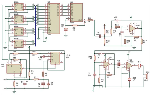
Schematic tools are software interfaces used to create diagrams that represent electrical circuits visually. They use standardized symbols for components like resistors, capacitors, and integrated circuits, connected by lines called nets to show signal flow. In PCB design for hobbyists, these tools matter because they catch errors early, saving time and materials compared to prototyping on breadboards alone. Without a proper schematic, transitioning to layout becomes chaotic, leading to routing mistakes or functional failures. Simple schematic tools make this step intuitive with drag-and-drop functionality and automatic labeling, ideal for those new to the field. Ultimately, they bridge the gap between conceptual sketches and manufacturable boards.
For hobbyists, the relevance extends to personal projects where quick iterations are key. A well-drawn schematic ensures compatibility with standard manufacturing processes, aligning with guidelines like IPC-2221 for generic printed board design principles. This standard emphasizes clear documentation, which even basic tools can support through netlists and bill of materials generation. By prioritizing schematics first, hobbyists reduce debugging time later, making the entire workflow more efficient.

Key Principles of Schematic Design
At the core of easy PCB design lies understanding symbols, which represent real-world components consistently across tools. Hobbyists should select libraries with common parts like passives and basic ICs, ensuring pins are accurately mapped for connectivity. Nets group connections logically, distinguishing power rails from signals to prevent confusion during layout. Buses simplify multi-bit signals, such as those in digital interfaces, by bundling lines neatly. Power and ground symbols designate dedicated planes, crucial for stable operation in any circuit.
Hierarchy adds structure for complex designs, breaking schematics into sheets that reference each other. This keeps diagrams readable, even as projects grow beyond single pages. Annotation with reference designators, values, and footprints links the schematic to physical placement. Following these principles ensures compliance with design standards, reducing risks like short circuits. Hobbyists benefit most by starting small, gradually incorporating these elements.
Adhering to IPC-2221 helps maintain signal integrity basics, such as proper decoupling near power pins. This standard outlines spacing and routing guidelines that start in the schematic phase.
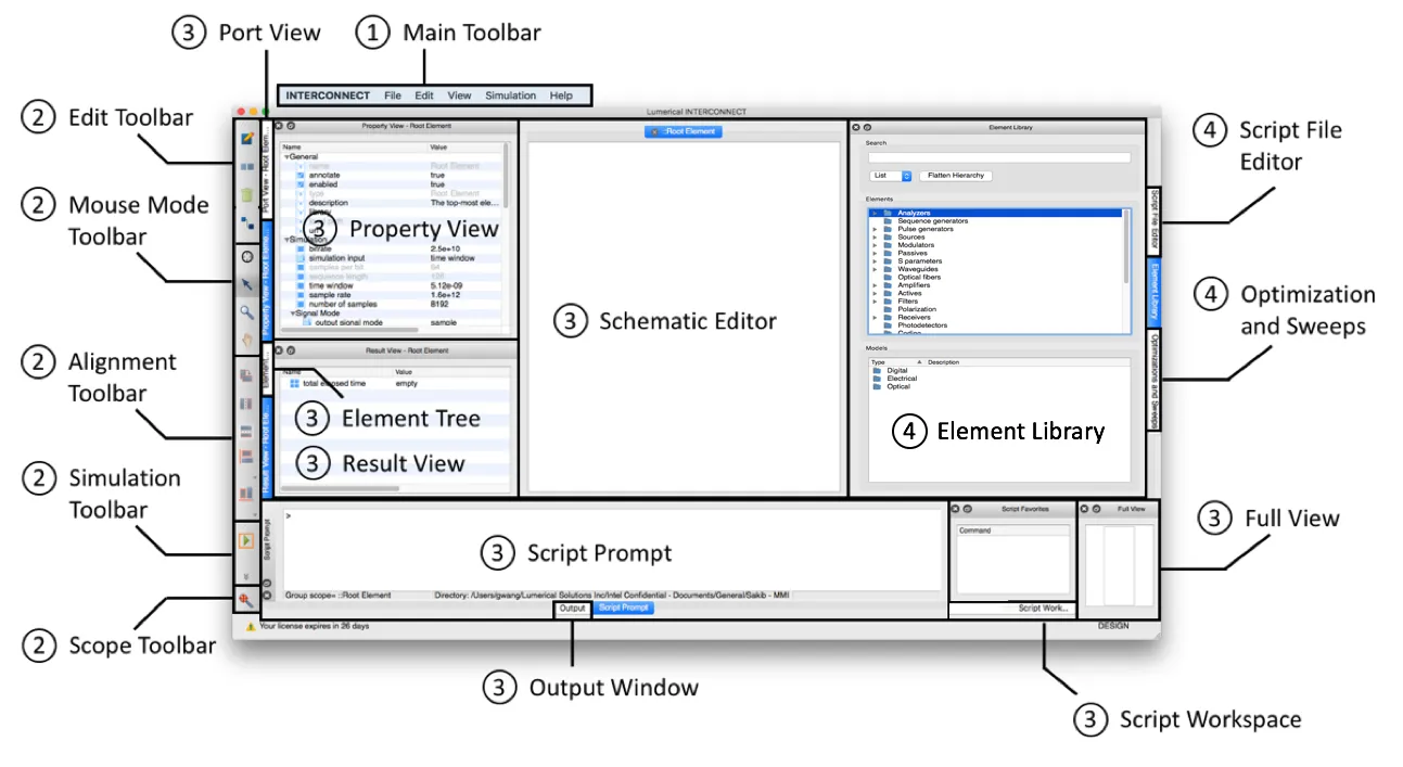
Features to Look for in Beginner PCB Design Software
When exploring beginner PCB design software, prioritize intuitive interfaces that minimize setup time. Drag-and-drop component placement speeds up initial drafting, while searchable libraries save hours hunting for symbols. Auto-numbering for references and net labels eliminates manual errors, a boon for those learning PCB design. Simulation integration, if available, lets you verify logic before committing to layout, catching issues like timing problems early.
Cross-probing between schematic and layout views fosters seamless workflow, helping hobbyists visualize transitions. Undo/redo stacks and zoom controls enhance usability during iterative tweaks. Export options for netlists and BOMs in standard formats ensure compatibility with fabrication services. Simple schematic tools shine with these features, making PCB design for hobbyists accessible without advanced training.
Step-by-Step Guide to Creating Schematics with Simple Schematic Tools
Begin your easy PCB design by defining project requirements, listing components needed for the circuit function. Open a new schematic in your chosen beginner PCB design software and place symbols from the library onto the sheet. Connect pins with net wires, using labels for distant points to keep lines clean and readable. Add power symbols for VCC and ground, ensuring every IC has bypass capacitors nearby.
Annotate components with values, tolerances, and footprints to generate a complete BOM. Run a design rule check (DRC) to flag unconnected pins or duplicate references. Update the netlist and forward it to the PCB layout editor. This structured approach teaches core skills while building functional designs.
For hobbyist projects like amplifiers or timers, test the schematic mentally or via basic simulation. Refine based on feedback, iterating until stable.
Best Practices for Effective Schematic Design
Keep schematics modular by grouping related functions into blocks, easing future modifications. Use consistent orientations for symbols to improve readability, aligning flows from left to right where possible. Label all nets explicitly, especially buses and power rails, to avoid ambiguity. Include test points and connectors early, planning for debugging access.
Document assumptions, like voltage levels or frequency ranges, in sheet notes. This practice aligns with J-STD-001 requirements for soldered assemblies, ensuring schematics support reliable builds. Hobbyists should version control files to track changes over time.
Minimize wire crossings by rerouting logically, preserving signal hierarchy. These habits make learn PCB design straightforward and scalable.
Common Mistakes in Beginner Schematics and How to Fix Them
A frequent error is forgetting decoupling capacitors, leading to noisy power supplies in operation. Always place 0.1 microfarad ceramics near each IC power pin, as per standard decoupling guidelines. Unlabeled nets cause routing confusion later, so apply unique names systematically. Overcrowded sheets hinder review, so employ hierarchy for anything beyond 50 components.
Missing ground returns create floating nodes, flagged by DRC tools. Double-check connectivity post-editing. Ignoring footprints mismatches components during layout, so select them during schematic entry. By addressing these proactively, hobbyists achieve robust easy PCB design outcomes.
Conclusion
Schematic tools transform PCB design for hobbyists from daunting to delightful, providing a clear path to functional boards. By grasping principles, leveraging simple schematic tools, and applying best practices, beginners can confidently tackle projects. Key takeaways include starting with requirements, using hierarchy for clarity, and running checks religiously. This foundation not only supports current hobbies but scales to more ambitious designs. Embrace the process, iterate freely, and watch your circuits come alive.
FAQs
Q1: What makes beginner PCB design software ideal for hobbyists?
A1: Beginner PCB design software excels with drag-and-drop interfaces, vast symbol libraries, and built-in DRC to simplify workflows. These features enable quick schematic creation without coding, perfect for learning PCB design basics. Auto-generated netlists and BOMs streamline the jump to layout, reducing errors common in manual drafting. Hobbyists appreciate simulation previews for validation before fabrication.
Q2: How do simple schematic tools support easy PCB design?
A2: Simple schematic tools focus on visual connectivity with nets and labels, making circuit logic transparent. They handle annotation and hierarchy automatically, keeping diagrams clean. Integration with layout prevents data loss, ensuring smooth progression. For hobbyists, this means faster prototyping of ideas like sensors or lights.
Q3: What are the first steps to learn PCB design using schematic software?
A3: Start by installing beginner-friendly software and exploring sample projects to familiarize with the interface. Sketch your idea on paper first, then digitize components and connections. Run DRC early and often to build good habits. Practice with basic circuits to master netlisting before complex builds.
Q4: Why prioritize schematics in PCB design for hobbyists?
A4: Schematics act as blueprints, verifying functionality before physical layout saves time and costs. They enforce standards like proper power distribution, minimizing assembly issues. Hobbyists gain debugging insights upfront, leading to reliable boards on the first try.
References
IPC-2221B — Generic Standard on Printed Board Design. IPC, 2009
J-STD-001G — Requirements for Soldered Electrical and Electronic Assemblies. IPC, 2011


