Introduction
Printed circuit board (PCB) design review is an essential process for anyone starting in electronics, especially electronic hobbyists venturing into their first custom boards. This PCB design review tutorial walks beginners through a structured approach to catch errors early, ensuring your beginner PCB design works as intended without costly reprints. Skipping this step often leads to issues like shorts, open circuits, or poor performance that could frustrate your projects. By following a systematic how to review PCB design method, you build confidence and reliability into your prototypes. Whether you're designing a simple Arduino shield or a sensor board, this guide provides clear, actionable steps tailored for hobbyists. Mastering these basics aligns your work with industry expectations right from the start.
What Is PCB Design Review and Why It Matters
PCB design review involves a thorough examination of your schematic, layout, and associated files to verify they meet functional, manufacturing, and reliability requirements. For beginners, it acts as a quality gate before fabrication, identifying issues like incorrect connections or inadequate clearances that might otherwise cause failures. This process matters because even small oversights in beginner PCB design can lead to board respins, wasting time and materials that hobbyists often work with limited budgets. In the hobbyist space, reliable boards enable experimentation with microcontrollers, sensors, and displays without constant troubleshooting. Regular reviews also foster good habits, preparing you for more complex projects. Ultimately, a solid how to review PCB design routine enhances project success rates and speeds up iteration cycles.
Key Technical Principles Behind Effective PCB Reviews
Understanding the core principles of PCB design helps frame your review effectively. Electrical connectivity starts with the schematic, where every net must connect components correctly without unintended paths. Layer stackup influences signal propagation and mechanical stability, requiring balanced copper distribution across planes. Thermal dissipation relies on copper pours and via stitching to spread heat from power components. Manufacturing tolerances, such as minimum trace widths and drill sizes, ensure producibility. Adhering to these principles prevents common pitfalls like voltage drops or electromagnetic interference in your beginner PCB design.
Signal integrity basics come into play even for hobbyists, where trace lengths affect timing in digital signals. Impedance matching, though advanced, begins with consistent routing widths. Power integrity demands stable ground returns to minimize noise. Mechanical considerations include board outline fits and mounting hole placements. These interconnected principles form the foundation of any PCB design review tutorial.
Step-by-Step Guide to Reviewing Your PCB Design
Step 1: Verify the Schematic Integrity
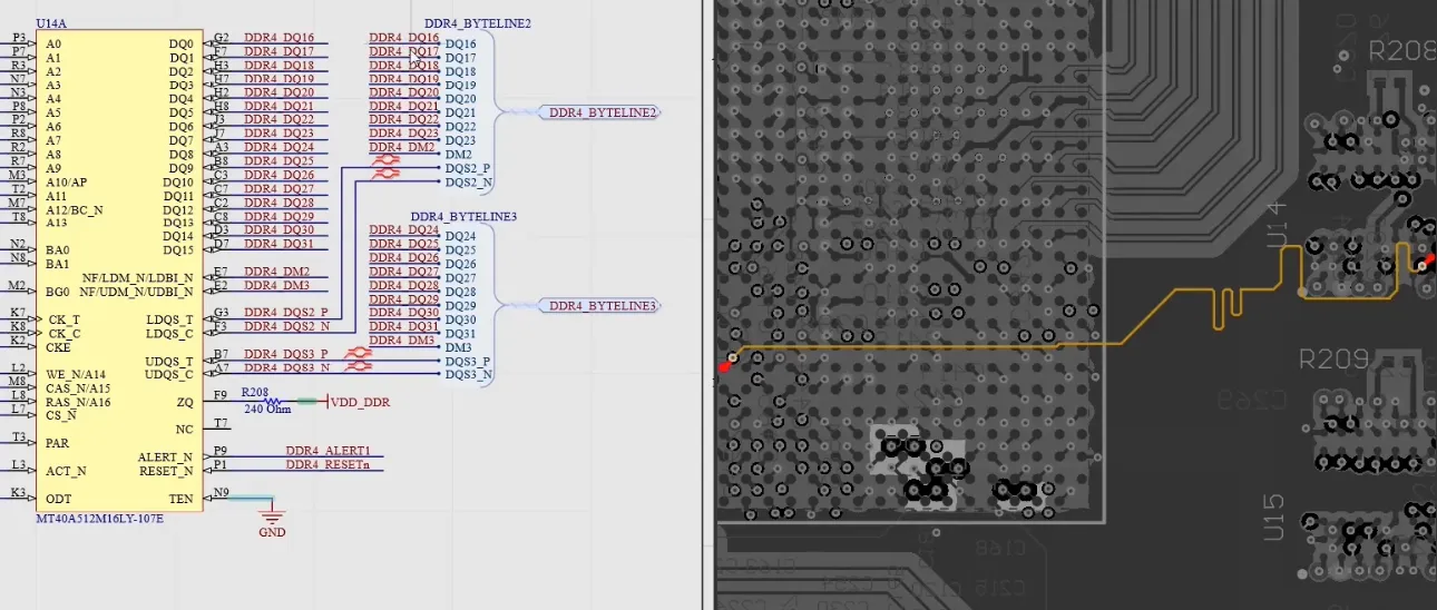
Begin your PCB design review tutorial with the schematic, the blueprint of your circuit. Check that all components match your bill of materials (BOM), confirming part numbers, values, and footprints align. Trace every net from power inputs to outputs, ensuring no floating pins or missing connections. Review decoupling capacitors near ICs to stabilize supply voltages. Simulate simple circuits if possible to catch logical errors early. This foundational step in how to review PCB design prevents downstream layout problems.
Look for power sequencing issues, like reset signals arriving before supplies stabilize. Confirm polarity on diodes, LEDs, and electrolytics to avoid reverse damage. Cross-reference with your project specs for voltage ratings and current limits. Annotate any discrepancies for fixes before proceeding. A clean schematic sets up successful beginner PCB design. A well-balanced multilayer configuration is essential for most beginner projects—refer to our dedicated guide on multilayer PCB design for beginners: creating your first multilayer board.
Step 2: Assess Component Placement
Once the schematic passes, evaluate component placement on the board layout. Group components by function, placing high-speed signals close to their drivers to minimize loop areas. Position heat-generating parts near edges or heatsinks, allowing airflow in enclosures. Separate analog and digital sections to reduce noise coupling. Ensure connectors and switches are accessible for user interaction. Mechanical fits, like battery holders or displays, must align with the board outline.
Prioritize signal flow from inputs to outputs for shorter paths. Avoid placing vias under large components that might interfere with soldering. Check for silkscreen labels that clearly identify test points and adjustments. This step in your PCB design review tutorial optimizes performance and ease of assembly.
Step 3: Inspect Routing and Traces
Routing demands careful attention in how to review PCB design. Verify trace widths meet current-carrying requirements, using wider paths for power rails to limit voltage drops. Space high-voltage traces from low-voltage ones to prevent arcing. Route critical signals on inner layers if multilayer, shielding them from crosstalk. Minimize vias in high-speed paths to reduce impedance discontinuities. Follow design rules for clearances, such as those outlined in IPC-2221 for generic printed board design.
Examine ground pours for complete fills without isolated islands. Check differential pairs for equal lengths and tight spacing. Avoid sharp 90-degree bends, opting for 45-degree angles to ease etching. Teardrops at vias strengthen connections against drill breakout. Thorough routing review ensures reliable signal transmission in beginner PCB design.
Step 4: Evaluate Power and Ground Planes
Power distribution is crucial; inspect planes for splits that create high-impedance paths. Stitch ground planes with vias to equalize potentials across layers. Place decoupling capacitors strategically, with short, wide traces to IC pins. Verify bulk capacitance near regulators for transient response. Flood unused areas with ground to improve shielding. These checks in your PCB design review tutorial maintain stable operation under load.
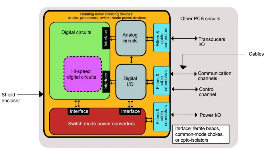
Monitor return paths for low inductance, routing them adjacent to signal traces. Separate analog and digital grounds, joining them at a single point near the power entry. Calculate plane thickness contributions to overall current capacity. This step prevents noise issues common in hobbyist prototypes.
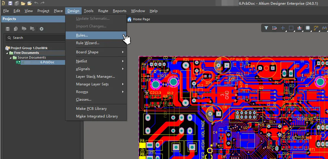
Step 5: Run Design Rule Checks (DRC)
Automated design rule checks (DRC) flag violations like insufficient clearances or overlapping pads. Set rules for minimum trace width, spacing, and via sizes based on your fab house capabilities. Review electrical rule checks (ERC) for unconnected pins or duplicate nets. Iterate fixes until zero errors remain. Manual spot-checks supplement automation for context-specific issues. DRC forms the backbone of any beginner PCB design review.
Step 6: Check Manufacturability and Assembly
Assess design for manufacturability (DFM) by ensuring panelization compatibility and fiducial marks for alignment. Minimum annular rings around pads must withstand drill tolerances. Solder mask expansion avoids bridging on fine-pitch parts. Test point access aids debugging post-assembly. Reference IPC-6012 for qualification specs on rigid boards to guide tolerances. These considerations in how to review PCB design streamline production.
For assembly, verify stencil-friendly pad shapes and no-hairpin vias under components. Include pull-up resistors if needed for unused inputs. Simulate reflow profiles mentally for lead-free processes. This holistic view catches fab-related errors early.
Step 7: Thermal and Reliability Analysis
Basic thermal review involves estimating junction temperatures via copper area calculators. Space hot components to avoid hotspots. Via thermal reliefs under pads improve heat sinking. For reliability, check creepage distances in humid environments. Humidity testing per J-STD-020 guidelines informs moisture sensitivity handling. These final checks complete your PCB design review tutorial.
Common Mistakes Beginners Make and How to Avoid Them
Hobbyists often overlook netlist mismatches between schematic and layout, causing dead circuits. Fix by regenerating the netlist post-schematic updates. Inadequate ground planes lead to noise; always prioritize solid pours. Ignoring fab minimums results in rejected jobs; consult stackup charts early. Rushing DRC without manual review misses context errors. Peer feedback catches blind spots effectively.
Overcrowded boards complicate soldering; allocate space for probes. Forgetting silkscreen polarity marks frustrates assembly. These pitfalls underscore the value of methodical how to review PCB design. For deeper insight into controlling these parameters, see our beginner-friendly overview of demystifying PCB signal integrity.
Tools and Resources for PCB Design Review
Free tools include KiCad’s built-in DRC/ERC, Gerbv for Gerber inspection, and online DFM checkers from manufacturers like Aivon or PCBWay. EasyEDA offers cloud-based rule checking with real-time collaboration.
Paid options such as Altium Designer provide advanced interactive DRC, signal integrity simulation, and thermal analysis. Free resources include IPC-2221 summaries, Zach Peterson's review videos, and Sierra Circuits'DFM guides.
To run automated checks: load your design rules file (most fabs provide one), run DRC/ERC, review the violation list, fix issues, and re-run until clean. Always verify outputs in a third-party viewer.
Best Practices for Ongoing Improvement
Develop a personalized checklist evolving with experience. Version control files to track changes. Simulate where tools allow for virtual testing. Join hobbyist forums for feedback, minus specifics. Review past boards post-build to refine processes. Consistent application elevates beginner PCB design to professional levels. Start with the fundamentals in our guide to high frequency PCB design for beginners once you have mastered basic design reviews.
Building Your Personal PCB Design Review Checklist
Use this comprehensive template and customize it. Copy into a Markdown file or spreadsheet for repeated use.
PCB Design Review Checklist Template
| Category | Item | Requirement/Example | Pass/Fail | Notes |
|---|---|---|---|---|
| Schematic | Component values & footprints match BOM | All parts verified against datasheet | ||
| Schematic | No floating pins or missing decoupling | 0.1 µF per IC + bulk caps | ||
| Layout/Stack-up | Symmetric stack-up with continuous GND plane | Reference planes adjacent to signals | ||
| Layout/Stack-up | Impedance targets met (50 Ω / 100 Ω diff) | Width/spacing calculated | ||
| Routing & SI | Trace widths adequate for current | 0.5 mm per 1 A on 1 oz | ||
| Routing & SI | Differential pairs length-matched within 10 mils | No excessive vias | ||
| Power/Thermal | Decoupling caps <10 mm from pins | Thermal vias under hot parts | ||
| DFM | Minimum annular ring ≥0.1 mm | Solder mask expansion 0.05–0.1 mm | ||
| DFM | Warpage control (symmetric copper) | Fiducials and tooling holes present | ||
| Documentation | Silkscreen readable and polarized | Gerbers verified in viewer |
Conclusion
This PCB design review tutorial equips you with a repeatable process to validate your beginner PCB design efforts. From schematic verification to DFM checks, each step builds toward reliable prototypes. Embracing standards like IPC guidelines ensures industry alignment. Regular practice reduces errors, accelerates projects, and sparks creativity in electronics. Start applying these today for frustration-free builds. Your next board will perform better than ever.
FAQs
Q1: What is a PCB design review tutorial for beginners?
A1: A PCB design review tutorial guides hobbyists through checking schematics, layouts, and rules to catch errors before fabrication. It covers steps like DRC, routing inspection, and DFM, ensuring functional boards. This process saves time and materials, making beginner PCB design accessible and reliable. Follow checklists for consistency.
Q2: How do I perform a basic how to review PCB design?
A2: Start with schematic nets, then placement, routing widths, and power planes. Run DRC for violations and manual checks for thermal issues. Verify manufacturability with clearances per standards. This structured how to review PCB design approach prevents common failures in prototypes. Iterate until clean.
Q3: Why is beginner PCB design review important for hobbyists?
A3: Beginner PCB design review identifies issues like shorts or noise early, avoiding respins that drain budgets. It promotes best practices for signal integrity and assembly ease. Reliable boards enable faster experimentation with sensors and controllers. Long-term, it builds skills for complex projects.
Q4: What standards help in PCB design review tutorial?
A4: Standards like IPC-2221 for design rules and IPC-6012 for board qualification provide benchmarks. They define trace spacing, vias, and tolerances for reliable outcomes. Incorporate them in your PCB design review tutorial to align with professional expectations. Reference during routing and DFM steps.
References
IPC-2221B — Generic Standard on Printed Board Design. IPC, 2003
IPC-6012E — Qualification and Performance Specification for Rigid Printed Boards. IPC, 2017
J-STD-020E — Moisture/Reflow Sensitivity Classification of Nonhermetic Surface Mount Devices. JEDEC, 2014


