Introduction
In RF applications, the PCB ground plane serves as the foundation for achieving reliable signal integrity and minimizing electromagnetic interference. Electric engineers designing circuits for wireless communication, radar systems, or high-speed data links must prioritize the RF PCB ground plane to ensure optimal performance at frequencies from hundreds of MHz to several GHz. Poor ground plane implementation leads to issues like signal distortion, increased noise, and radiation emissions that fail regulatory compliance. This article explores key design considerations, including the RF signal return path and high-frequency grounding techniques, to guide engineers toward robust layouts. By understanding these principles, designers can create PCBs that maintain low loss and high efficiency.
What Is an RF PCB Ground Plane and Why It Matters
An RF PCB ground plane consists of a continuous copper layer that acts as a low-impedance reference for signal traces and components operating at radio frequencies. Unlike low-frequency designs where ground acts merely as a return for DC currents, in RF contexts, it forms the primary path for high-frequency return currents due to the skin effect concentrating currents on conductor surfaces. This plane also shields sensitive signals from external noise and prevents unintended radiation from trace loops. Engineers must recognize that the ground plane directly influences ground plane impedance RF, which if uncontrolled, causes reflections and standing waves that degrade performance.
The importance of a well-designed RF PCB ground plane becomes evident in maintaining characteristic impedance along transmission lines like microstrips or striplines. At high frequencies, return currents seek the path of least inductance, hugging the ground plane directly beneath the signal trace. Disruptions such as slots or voids force currents to detour, increasing loop inductance and EMI susceptibility. Proper implementation reduces crosstalk between adjacent traces and supports RF grounding techniques that comply with industry expectations for signal integrity. Ultimately, a solid ground plane enhances overall system reliability in demanding RF environments.
Technical Principles Behind RF Ground Planes
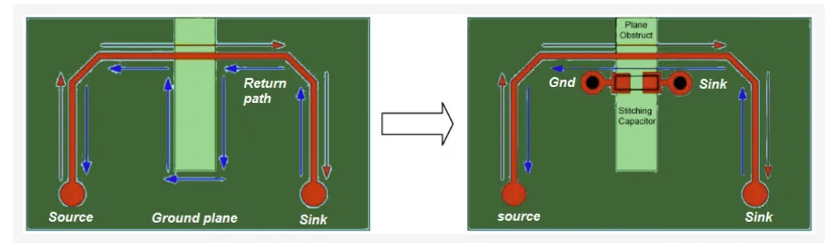
The core principle governing RF PCB ground planes revolves around the RF signal return path, where high-frequency currents flow back to the source via the nearest low-impedance route rather than a distant chassis ground. At RF frequencies, electromagnetic fields propagate as guided waves between the signal trace and its image in the ground plane, forming a transmission line structure. Skin effect limits current penetration to microns in copper, making the ground plane's surface quality critical for minimizing losses. Proximity effects further concentrate return currents under the trace, emphasizing the need for uninterrupted plane continuity.
Ground plane impedance RF arises from the plane's effective series inductance and resistance, which scale inversely with area but increase with perforations or splits. Large, solid planes distribute currents broadly, achieving sub-ohm impedances at GHz frequencies, while grids or hatched patterns introduce higher inductance due to current crowding at crossings. Displacement currents through dielectrics also contribute at very high frequencies, requiring symmetric stackups to balance fields. These mechanisms underscore why high-frequency grounding demands planes that approximate an ideal zero-potential reference.
Engineers must consider radiation from unbalanced transmission lines, where asymmetric fields couple to free space if the ground plane fails to contain them. Boundary conditions at plane edges can cause edge resonances, mitigated by extending the plane beyond signal extents. Thermal expansion mismatches in multi-layer boards can warp planes, altering spacing and impedance, so adherence to standards like IPC-2221 for material and layout guidelines proves essential. Understanding these principles enables predictive modeling of performance before fabrication.
Design Considerations for Optimal RF Ground Plane Performance
Selecting the layer stackup represents the first critical step in RF PCB ground plane design, with signal layers sandwiched between dedicated ground planes to minimize inductance. Four-layer boards suffice for many applications, placing RF signals on outer layers over inner grounds, while eight-layer or more suit complex mixed-signal designs. Dielectric thickness controls characteristic impedance, typically targeting 50 ohms for single-ended lines, with thinner dielectrics enabling tighter coupling. Ground plane thickness, often 1 to 2 oz copper, balances current capacity and skin effect losses without excessive cost.
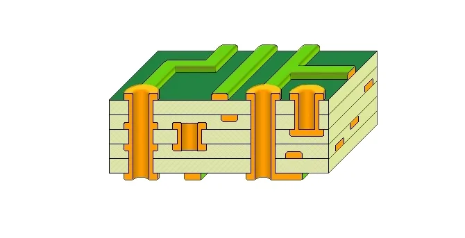
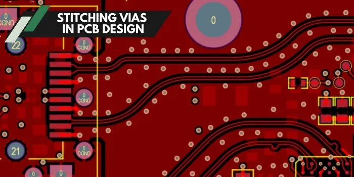
Maintaining plane continuity avoids slots or moats that cross perpendicular to signal traces, as these force return currents to detour via higher-inductance paths. In partitioned designs for analog and digital sections, bridges or stitching vias connect grounds at multiple points to equalize potentials. RF grounding techniques include via fences around sensitive areas, spaced at one-twentieth of the wavelength or closer for GHz signals, forming shielded enclosures. Clearance rules prevent shorts while allowing field containment.
Component placement influences ground plane effectiveness, positioning RF ports and matching networks directly over solid copper to shorten return loops. Decoupling capacitors bridge power to ground with minimal via stubs, using arrays for broadband response. For embedded antennas, ground plane shape affects radiation patterns, often requiring cutouts simulated iteratively. High-frequency grounding further benefits from coplanar waveguide structures, where ground extends alongside traces on the same layer for distributed capacitance.
Fabrication tolerances impact ground plane impedance RF, with plating variations altering surface roughness and thus losses. Etch factors ensure uniform copper removal, while solder mask over planes adds minor capacitance without bridging risks. Multi-layer registration aligns vias precisely to prevent plane discontinuities. Following IPC-6012 qualification specs verifies plane integrity post-manufacture through electrical testing.
Best Practices and High-Frequency Grounding Techniques
Implement solid copper pours rather than grids for RF PCB ground planes, as grids elevate inductance by factors of ten or more at high frequencies. Pour grounds on all non-signal layers where possible, connecting them densely with through-vias to form a unified reference. For mixed-signal boards, single-point connections at power entry minimize loops, transitioning to meshed planes away from RF zones. Simulate return paths using field solvers to visualize current density and optimize layouts preemptively.
RF grounding techniques emphasize via optimization: blind or buried vias reduce stubs, while back-drilling clears unused portions for lower reflections. Place ground vias every quarter-wavelength along trace bends to preserve impedance continuity. Power planes pair with ground planes through interplane capacitors for low-inductance decoupling at RF. Thermal reliefs in ground vias aid assembly without compromising RF performance.
Troubleshoot common issues by inspecting for voids under hot spots, using X-ray for inner layers. Excessive ground bounce signals poor stitching; add more vias iteratively. EMI scans reveal plane resonances, resolved by absorbers or reshaping. These practices align with J-STD-001 requirements for soldered connections in high-reliability assemblies.
Case Insights: Optimizing Ground Planes in Multi-GHz Designs
Consider a typical 5G mmWave module where initial prototypes suffered 10 dB insertion loss due to split grounds under mmWave traces. Redesigning with contiguous inner planes and λ/20 via stitching restored flat response to 28 GHz. Simulations confirmed return currents stayed confined, dropping radiated emissions below limits. Such insights highlight proactive stackup planning over reactive fixes.
Another scenario involves radar PCBs with phased arrays, where ground plane edges diffracted beams. Extending planes 3λ beyond array edges and adding fence vias sharpened patterns. These examples demonstrate logical progression from principles to verified performance.
Conclusion
Effective RF PCB ground plane design hinges on providing a low-impedance RF signal return path through solid, continuous copper layers adjacent to signals. Key considerations like stackup symmetry, via stitching, and avoiding discontinuities directly control ground plane impedance RF and support high-frequency grounding techniques. Engineers applying these structured approaches achieve superior signal integrity, reduced EMI, and compliance with standards. Prioritizing these elements from concept through fabrication ensures RF applications deliver peak performance reliably.
FAQs
Q1: What role does the RF signal return path play in PCB ground plane design?
A1: The RF signal return path follows the lowest inductance route on the ground plane directly under the signal trace, critical at high frequencies due to skin and proximity effects. Disruptions increase loop area, causing radiation and crosstalk. Solid RF PCB ground planes minimize this path length, preserving impedance and reducing losses. Proper design confirms currents remain contained for optimal performance.
Q2: How do you control ground plane impedance RF in high-frequency applications?
A2: Ground plane impedance RF lowers with larger areas and smoother surfaces, avoiding grids or splits that raise inductance. Use dedicated planes adjacent to signals with controlled dielectric spacing for balanced fields. Stitching vias connect planes, distributing currents evenly. Simulations validate low effective impedance below 0.1 ohms at GHz bands.
Q3: What are essential RF grounding techniques for multi-layer PCBs?
A3: Key RF grounding techniques include via fences spaced at λ/20, solid pours without slots under traces, and symmetric stackups with ground-signal-ground layering. Decouple power to ground densely near RF components. Partition mixed signals with bridged connections to prevent loops. These ensure low-impedance references across frequencies.
Q4: Why avoid splits in RF PCB ground planes?
A4: Splits force return currents to longer paths, elevating inductance and causing reflections or EMI. In high-frequency grounding, they disrupt field containment, radiating energy. Continuous planes maintain uniform potential, supporting precise impedance control. Bridge only when necessary with multiple vias.
References
IPC-2221B — Generic Standard on Printed Board Design. IPC, 2003
IPC-6012E — Qualification and Performance Specification for Rigid Printed Boards. IPC, 2015
J-STD-001G — Requirements for Soldered Electrical and Electronic Assemblies. IPC, 2017


