Introduction
Thermal reliefs play a critical role in PCB footprint thermal design, balancing the need for efficient soldering heat dissipation with effective PCB thermal management. These features address the challenge of heat sinking by large copper planes during assembly, preventing incomplete reflow and cold solder joints. Engineers often encounter difficulties when through-hole pins or surface-mount pads connect directly to expansive copper areas, as the rapid heat dissipation hinders solder melting. By incorporating thermal reliefs, designers ensure reliable joints while maintaining electrical connectivity. This article explores the principles, implementation, and best practices for thermal reliefs in PCB footprints, drawing on established engineering approaches for electric engineers.
What Are Thermal Reliefs and Why Do They Matter in PCB Design?
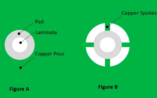
Thermal reliefs are intentional gaps or spoke-like connections between a solder pad and an adjacent copper plane or thick trace in a PCB footprint. They limit thermal conductivity during soldering, allowing localized heat buildup for proper solder reflow. Without them, the plane acts as a massive heat sink, drawing away heat faster than it can melt the solder, leading to poor wetting and joint reliability. This issue is particularly pronounced in hand soldering, rework, or wave soldering processes where controlled heat application is essential.
In modern PCB thermal management, thermal reliefs contribute to overall assembly success rates. They align with soldering heat dissipation requirements by enabling consistent temperatures at the joint interface. Industry standards like IPC-7351B outline specific geometries for these features to optimize land patterns. For electric engineers, understanding thermal reliefs ensures designs meet performance criteria without compromising manufacturability.
The Physics of Heat Transfer in PCB Footprints
Heat transfer during soldering follows principles of conduction, primarily governed by Fourier's law, where flux is proportional to the temperature gradient and material cross-section. A direct pad-to-plane connection maximizes conductive paths, resulting in high thermal conductance that dissipates input energy across the plane. Thermal reliefs introduce narrow spokes or gaps that reduce the effective cross-sectional area, increasing thermal resistance and confining heat to the pad. This controlled isolation promotes uniform solder melting and intermetallic formation.
Copper's high thermal conductivity, around 400 W/m·K, exacerbates heat sinking in plane connections. Spoke width, typically comparable to trace widths, and the number of spokes (often three or four) determine the relief's effectiveness. Gaps prevent bridging while allowing post-soldering thermal paths for operational heat dissipation. Engineers must model these effects, considering solder alloy properties like Sn63/Pb37 with melting points near 183°C.
Reflow profiles further influence dynamics, with peak temperatures of 220-260°C for lead-free processes. Thermal reliefs ensure pads reach these thresholds without excessive dwell times that risk delamination. In multilayer boards, inner plane connections amplify challenges, necessitating reliefs on all layers.
Types of Thermal Reliefs in PCB Footprints
Thermal reliefs come in spoke-style and windowed configurations, each suited to specific applications. Spoke-style reliefs use radial copper bridges, providing mechanical strength and electrical continuity post-soldering. Windowed reliefs employ a clearance gap around the pad, fully isolating it thermally during assembly. Selection depends on pin type, plane thickness, and assembly method.
For through-hole technology (PTH), spokes are standard, connecting the annular ring to the plane. Surface-mount devices (SMD) with exposed pads, like QFNs, use similar patterns or hatched fills for thermal pads. IPC-2221B provides guidance on conductor widths and spacings to balance thermal and electrical performance. Engineers evaluate trade-offs, as reliefs slightly elevate junction temperatures under load.
Best Practices for PCB Footprint Thermal Design with Reliefs
Start by identifying pads connected to planes wider than three times the pad diameter, mandating reliefs per design guidelines. Use three or four spokes with widths matching signal trace dimensions, around 0.1-0.2 mm for fine-pitch boards. Ensure spoke gaps of 0.2-0.3 mm to avoid solder bridging during reflow. Verify symmetry for uniform heating.
In PCB thermal management, simulate heat flow using finite element analysis to quantify relief impact. For high-power components, supplement with vias under the pad for post-assembly spreading. During layout, apply reliefs consistently across libraries to streamline fabrication. Test prototypes with thermal cameras to confirm joint formation.
Adhere to IPC J-STD-001 requirements for solder joint fillet formation and wetting. Adjust for board thickness and copper weight, as 2-oz planes demand wider gaps. Document relief parameters in fabrication notes for consistency.
Related Reading: Thermal Relief: Optimizing Pad Connections for Soldering and Heat Dissipation
Balancing Soldering Heat Dissipation and Operational Thermal Performance
Thermal reliefs optimize soldering but introduce minor thermal impedance during operation, raising concerns for power dissipation. In high-current paths, this resistance can limit heat spreading, potentially exceeding component ratings. Mitigate by using multiple spokes or direct-connecting non-soldered thermal vias. For RF or high-speed signals, reliefs preserve integrity without plane stubs.
Compare direct connects versus reliefs: direct offers lowest resistance but risks assembly defects; reliefs prioritize reliability. In volume production with vapor phase or selective soldering, minimal reliefs suffice. Engineers prioritize based on assembly process, using risk analysis for hybrids.
Related Reading: Component Footprints for SMT Assembly: Optimizing for Pick and Place Machines
Troubleshooting Common Issues in Thermal Relief Implementation
Incomplete reflow manifests as dull, concave joints from excessive heat sinking. Verify spoke dimensions and increase gap size if persistent. Overly wide spokes mimic direct connects, causing cold joints; narrow them iteratively. Inspect for fab variations in etch tolerances affecting relief gaps.
Post-assembly failures like cracking arise from thermal cycling mismatch. Reliefs reduce soldering stress but monitor operational temps. Use X-ray for hidden joints in BGAs with thermal pads. Adjust designs based on yield data from first articles.
Conclusion
Thermal reliefs are indispensable in PCB footprint thermal design, ensuring soldering heat dissipation without sacrificing joint integrity. By interrupting direct heat paths, they enable reliable reflow while supporting PCB thermal management goals. Engineers benefit from structured application of spokes and gaps, guided by standards like IPC-7351B. Integrating simulations and prototypes refines implementations for diverse assemblies. Prioritizing these features enhances yield, reduces rework, and upholds design robustness.
FAQs
Q1: What is a thermal relief PCB and when should it be used?
A1: A thermal relief PCB feature consists of spoke connections in footprints to limit heat sinking during soldering. Use them for any pad linked to copper planes or thick traces exceeding pad width significantly. This prevents cold joints in hand or wave soldering, aligning with PCB footprint thermal design best practices. Without reliefs, heat dissipates too quickly, compromising wetting.
Q2: How do thermal reliefs improve soldering heat dissipation?
A2: Thermal reliefs confine heat to the pad by reducing conductive cross-section, allowing solder to reach reflow temperature efficiently. Spokes provide balance between assembly ease and electrical paths. In PCB thermal management, they ensure consistent profiles across components. Adjust spoke count and width based on plane size for optimal results.
Q3: Are thermal reliefs necessary for reflow soldering in PCB thermal management?
A3: While less critical in conveyor reflow due to uniform heating, thermal reliefs aid rework and prevent defects in mixed assemblies. They standardize footprints per IPC guidelines. For lead-free processes with higher peaks, reliefs mitigate plane-induced gradients. Always include for versatility.
Q4: What are common mistakes in implementing thermal relief PCB designs?
A4: Overly narrow spokes cause fragility; too wide defeats the purpose. Inconsistent application across layers leads to uneven heating. Neglecting simulation overlooks operational impacts on heat dissipation. Follow structured checks and standards for reliable outcomes.
References
IPC-7351B — Generic Requirements for Surface Mount Design and Land Pattern Standard. IPC, 2010
IPC-2221B — Generic Standard on Printed Board Design. IPC, 2003
IPC J-STD-001H — Requirements for Soldered Electrical and Electronic Assemblies. IPC, 2018


