Introduction
In high-speed PCB designs, maintaining precise signal timing is essential for reliable operation. Jitter introduces timing uncertainties that degrade PCB signal integrity, leading to bit errors and system failures. Electrical engineers face increasing challenges as data rates climb into gigabits per second, where even picoseconds of deviation matter. This guide explores PCB design jitter comprehensively, from its sources to measurement and mitigation strategies. By understanding jitter sources in PCB layouts and applying targeted best practices, designers can achieve robust signal integrity. Whether working on clock distribution networks or data buses, minimizing jitter ensures compliance with performance margins and enhances overall board reliability.
What Is Jitter and Why It Matters in PCB Design
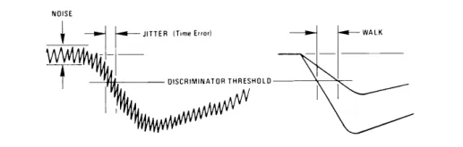
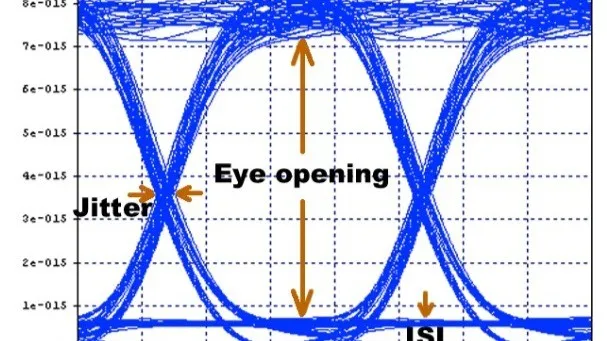
Jitter refers to the deviation of a signal's edge from its ideal position in time, manifesting as short-term variations in digital waveforms. In PCB contexts, it encompasses both random components, driven by thermal noise, and deterministic ones from reflections or crosstalk. Period jitter measures cycle-to-cycle differences, while phase jitter tracks long-term accumulation relative to a reference clock. These variations close the eye diagram, reducing timing margins and increasing bit error rates in high-speed links. For electrical engineers, PCB design jitter directly impacts setup and hold times, potentially violating critical paths in processors or memory interfaces. Neglecting jitter compromises PCB signal integrity, resulting in intermittent failures that are hard to diagnose during prototyping.
The relevance intensifies in modern applications like 5G, AI accelerators, and automotive electronics, where clock frequencies exceed several gigahertz. Excessive jitter amplifies inter-symbol interference, degrading eye height and width. Engineers must prioritize jitter early in the layout phase to avoid costly respins. Quantifying its effects through simulations reveals how it propagates across the board, influencing downstream receivers. Ultimately, effective jitter management upholds system-level performance and meets stringent industry timing budgets.
Primary Jitter Sources in PCB Layouts
Power supply noise stands as a dominant jitter source in PCB designs, where voltage ripples couple into sensitive clock lines. Transients from switching regulators or load changes induce ground bounce, modulating edge timings. Decoupling capacitors mitigate this partially, but poor placement exacerbates the issue. In multi-layer boards, shared return paths amplify these effects, turning PDN impedance peaks into jitter contributors.
Crosstalk emerges from aggressive routing densities, where aggressor signals induce voltage glitches on victims via capacitive or inductive coupling. Adjacent high-speed traces without sufficient spacing transfer energy, peaking near parallel runs longer than a wavelength fraction. This deterministic jitter appears periodic, aligning with aggressor frequencies. Engineers observe it prominently in DDR or PCIe lanes, where mutual inductance distorts rise times.
Reflections due to impedance discontinuities rank high among jitter sources in PCB interconnects. Vias, bends, or unterminated stubs create echoes that smear edges, introducing data-dependent jitter. Unmatched trace widths or layer transitions compound this, especially beyond 1 GHz. Transmission line theory dictates that return loss below 10 dB generates measurable deterministic jitter.
Clock generator imperfections contribute intrinsic jitter, propagated through distribution trees. Oscillator phase noise converts to timing errors under load. PCB parasitics like stub lengths further degrade this baseline. Environmental factors, such as EMI from nearby sources, add random components.
Dielectric absorption and skin effect introduce subtle jitter at very high frequencies, though less dominant than noise coupling. Cumulative effects from multiple sources necessitate holistic analysis.
Clock Jitter Measurement Techniques
Accurate clock jitter measurement begins with eye diagram analysis, visualizing timing uncertainty across thousands of cycles. Engineers overlay multiple acquisitions to assess jitter bounds, identifying bathtub curves for total jitter projections. This method reveals both random and deterministic components qualitatively.
For quantitative assessment, period jitter calculation per JEDEC JESD65B involves sampling at least 10,000 cycles, computing deviations from the mean period. High-bandwidth oscilloscopes capture edge positions relative to a trigger, yielding RMS or peak-to-peak values. Cycle-to-cycle jitter focuses on adjacent periods, sensitive to local noise.
Time interval error provides phase noise decomposition, using PLL references for absolute timing. Spectral analysis via FFT isolates periodic jitter peaks. Pre-layout simulations predict these metrics, guiding iterations.
Validation post-fabrication confirms PCB signal integrity, correlating measurements to design margins. Threshold settings at 50% ensure repeatability across tools.
Best Practices for Reducing Jitter in PCBs
Optimize the power distribution network first, placing high-frequency decoupling capacitors within millimeters of clock pins. Solid planes minimize impedance below 1 GHz, suppressing ripple below 50 mV. Segregate analog and digital supplies to prevent cross-domain noise.
Follow IPC-2221 guidelines for trace routing, maintaining 3W spacing rules for high-speed signals to curb crosstalk. Use differential pairs with tight length matching within 0.5 mil for clocks. Avoid right-angle bends, opting for 45-degree miters to preserve impedance.
Controlled impedance stackups, verified via field solvers, prevent reflections. Symmetric layer builds with low-loss dielectrics like FR-4 variants reduce attenuation. Dedicate inner layers to ground for return current paths.
Shield sensitive nets with guard traces or stitching vias, grounded at both ends. Enclose clock trees in ground cages to block EMI ingress.
Length-tune clock distribution for skew minimization, targeting sub-picosecond differences. Source-synchronous schemes with forwarded clocks inherently tolerate jitter.
Terminate lines appropriately, using series or parallel resistors matched to characteristic impedance. AC coupling capacitors filter low-frequency wander.
Partition the layout logically, isolating noisy sections with moats or split planes tied at single points. Simulate PDN and S-parameters pre-layout to quantify jitter budgets.
Employ via-in-pad or blind vias sparingly, optimizing stub lengths below quarter-wavelength. Thermal management prevents drift from hotspots.
Troubleshooting Jitter Issues in High-Speed Designs
Suspect power noise first by probing PDN rails with spectrum analyzers. Spikes correlating to clock harmonics indicate coupling paths. Add bulk capacitance iteratively.
Crosstalk manifests in near-end/ far-end diagrams; widen spacing or add shielding. Reflections show as ringing; TDR confirms discontinuities.
Eye closure beyond specs prompts de-embedding channel losses. Correlate simulations to hardware, adjusting models.
IPC-6012 performance specs guide qualification, ensuring fabricated boards meet integrity thresholds.
Conclusion
Minimizing jitter demands integrated efforts across stackup, routing, and PDN design. Addressing jitter sources in PCB early prevents signal integrity pitfalls. Clock jitter measurement validates strategies, aligning with standards like JEDEC JESD65B. Implementing best practices yields robust high-speed boards. Electrical engineers benefit from structured approaches, ensuring timing margins for next-generation systems.
FAQs
Q1: What are the main jitter sources in PCB layouts?
A1: Power supply noise, crosstalk from adjacent traces, and reflections from impedance mismatches top the list of jitter sources in PCB designs. Ground bounce and EMI further contribute random and deterministic components. Proper PDN design and spacing rules mitigate these effectively. Simulations help quantify impacts before fabrication.
Q2: How can engineers measure clock jitter in PCBs?
A2: Clock jitter measurement relies on eye diagrams and period analysis over 10,000 cycles as per JEDEC JESD65B. Oscilloscopes capture edge deviations, computing RMS values. Spectral methods isolate components. This ensures PCB signal integrity meets budgets. Post-layout probing confirms predictions.
Q3: What best practices reduce jitter in PCB designs?
A3: Key practices include controlled impedance routing, decoupling near clocks, and ground plane shielding for reducing jitter in PCBs. Length matching and termination prevent reflections. PDN optimization suppresses noise. Following IPC-2221 spacing enhances integrity. Holistic simulation verifies results.
Q4: Why does PCB design jitter affect signal integrity?
A4: PCB design jitter erodes eye opening, violating setup/hold times and raising BER. It accumulates from multiple sources, closing timing windows. High-speed links amplify effects. Mitigation preserves margins, ensuring reliable data transfer. Standards guide acceptable levels.
References
JEDEC JESD65B — Definition of Definitions of Terms for Jitter. JEDEC.
IPC-2221B — Generic Standard on Printed Board Design. IPC, 2012.
IPC-6012E — Qualification and Performance Specification for Rigid Printed Boards. IPC, 2015.


