Introduction
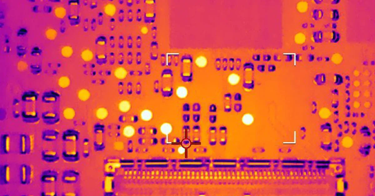
High-power PCBs in applications like power supplies, motor drives, and RF amplifiers face significant thermal challenges. Excessive heat from components such as MOSFETs and voltage regulators can lead to performance degradation, reduced lifespan, and outright failure. Thermal via stitching emerges as a critical technique to manage this heat effectively. By creating pathways for heat to spread across multiple layers, it enhances overall PCB heat dissipation via stitching. This approach is essential for electric engineers designing reliable systems in power electronics. Mastering thermal via stitching best practices ensures boards meet demanding thermal requirements without relying solely on bulky heatsinks.
What Is Thermal Via Stitching and Why It Matters
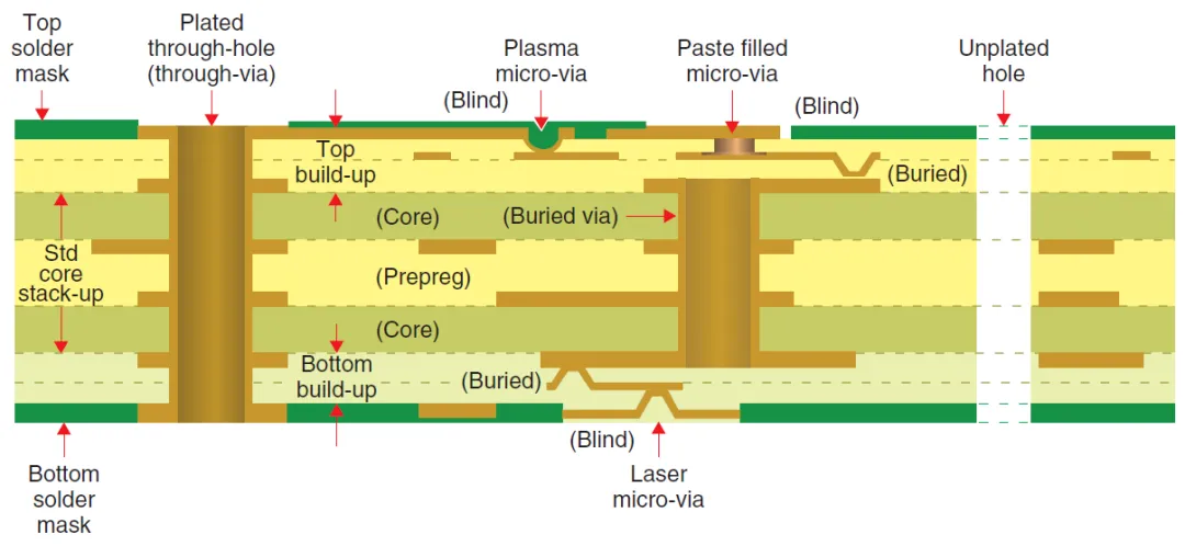
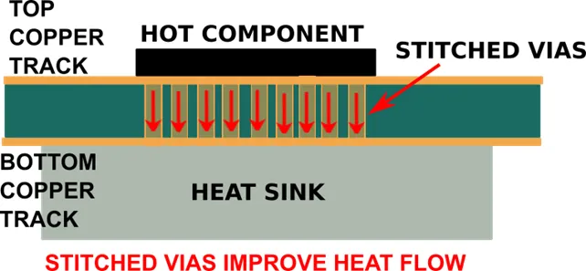
Thermal via stitching involves placing an array of closely spaced vias under or near heat-generating components to conduct heat vertically through the PCB stackup. These vias connect the top copper layer, where the component sits, to inner ground or power planes that act as heat spreaders. Unlike single thermal vias, stitching uses multiple vias in a grid pattern to increase the effective thermal cross-section and reduce thermal resistance. This method is particularly vital for via stitching for power electronics, where current densities exceed standard designs.
The importance lies in preventing localized hotspots that exceed component junction temperatures. In high-power scenarios, poor heat management violates reliability standards and accelerates electromigration. Effective stitching aligns with IPC-2221 guidelines for via design, promoting uniform temperature distribution. Engineers benefit from lower thermal gradients, which improve signal integrity and mechanical stability across the board.
Technical Principles of Thermal Via Stitching
Heat transfer in stitched vias primarily occurs through conduction along the copper plating inside the via barrel. The thermal conductivity of copper, combined with the plating thickness typically around 1 ounce per square foot, determines the via's effectiveness. Multiple vias in parallel reduce the overall thermal resistance, following the principle that thermal conductance is proportional to the total cross-sectional area. Filling vias with conductive epoxy or copper electroplating further boosts performance by minimizing air gaps that impede heat flow.
The PCB stackup plays a crucial role, as inner planes provide lateral spreading. Heat flows from the component pad through the vias to these planes, then dissipates outward. Tenting the vias on non-component sides prevents solder wicking during assembly, preserving the thermal path. Simulations using finite element analysis reveal optimal configurations, ensuring compliance with thermal performance expectations in IPC-2152 for current-related heating.
Via geometry affects outcomes significantly. Smaller diameter vias allow denser arrays but limit plating thickness, while larger ones offer better conductance at the cost of board space. Aspect ratio, governed by fabrication capabilities, influences plating uniformity and void formation. Engineers must balance these factors with the board's overall thermal budget.
PCB Heat Dissipation via Stitching: Key Mechanisms
Effective PCB heat dissipation via stitching relies on interconnecting multiple copper layers for three-dimensional heat flow. Ground planes on inner layers serve as primary sinks, distributing heat away from hotspots. The stitching density determines the heat transfer rate, with closer spacing yielding lower resistance paths. In power electronics, this mechanism supports higher current handling without excessive temperature rise.
Convection and radiation contribute marginally compared to conduction in dense arrays. However, exposed planes on the bottom side enhance natural airflow cooling. During operation, steady-state temperatures stabilize faster with stitching, reducing transient thermal stress on components. This aligns with J-STD-001 requirements for soldered connections under thermal loads.
Thermal Via Stitching Best Practices
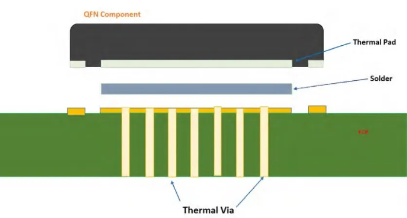
Follow thermal via stitching best practices by simulating thermal performance early in the design phase. Place vias directly under the thermal pad of components like QFNs or LQFP packages with exposed pads. Use a grid pattern with pitch spacing that maintains drill-to-drill clearances per fabrication rules. Connect every via to solid copper pours on all layers to maximize spreading.
Opt for via diameters between 0.2 mm and 0.4 mm for high-density boards, ensuring plating covers at least 75% of the barrel. Tent solder mask over vias on the component side to avoid solder voids, and consider filling for extreme cases. Verify array coverage spans the entire heat source footprint, avoiding edges where fringing reduces efficiency. These steps embody PCB heat dissipation via stitching principles for robust designs.
Incorporate stitching along high-current traces every few millimeters to aid both thermal and electrical distribution. Avoid placing vias too close to sensitive signals to prevent crosstalk. Post-layout thermal analysis confirms junction temperatures stay below datasheet limits. Adhering to these practices supports via stitching for power electronics in demanding environments.
Common Challenges and Troubleshooting
Engineers often encounter solder wicking into untented vias, which plugs the thermal path. Mitigate this by applying solder mask plugs or specifying filled vias during fabrication. Voids in plating from high aspect ratios degrade conductance, so limit ratios to 6:1 or less. Inspect arrays via X-ray for uniformity post-assembly.
Another issue is mechanical stress from CTE mismatch in multi-layer boards, leading to via cracking under thermal cycling. Use controlled impedance planes and symmetric stackups to minimize warpage. If hotspots persist, increase via count or add microvias for finer pitch. Troubleshooting involves iterative simulation and prototyping.
Conclusion
Thermal via stitching stands as a cornerstone for cooling high-power PCBs, enabling efficient heat transfer across layers. By implementing structured arrays under heat sources, engineers achieve superior PCB heat dissipation via stitching. Key to success are simulations, proper geometry, and alignment with standards like IPC-2221 and IPC-2152. Via stitching for power electronics not only boosts reliability but also allows compact designs. Prioritize these techniques to deliver boards that perform under thermal stress.
FAQs
Q1: What are thermal via stitching best practices for high-power components?
A1: Thermal via stitching best practices include placing a dense grid of 0.3 mm diameter vias under thermal pads, with pitch around 1 mm, connected to inner planes. Tent vias to prevent solder wicking and simulate for uniform heat spread. Filling enhances performance in extreme cases. This ensures reliable PCB heat dissipation via stitching without excessive board area.
Q2: How does PCB heat dissipation via stitching improve power electronics designs?
A2: PCB heat dissipation via stitching transfers heat vertically to spreading planes, reducing hotspot temperatures by up to 30% in simulations. It supports higher currents by lowering thermal resistance in parallel paths. Essential for MOSFETs and regulators, it prevents derating. Combine with copper pours for optimal results in via stitching for power electronics.
Q3: When should you use via stitching for power electronics?
A3: Use via stitching for power electronics when component power exceeds 1 W or junction temperatures approach limits. Ideal for multi-layer boards with exposed pad packages. It excels in applications like DC-DC converters needing compact thermal management. Avoid in low-power signals to save space.
Q4: What role do standards play in thermal via stitching?
A4: Standards like IPC-2221 guide via dimensions and protection for thermal paths, while IPC-2152 informs current-temperature modeling. They ensure designs meet qualification for reliability. J-STD-001 addresses assembly impacts on vias. Following them standardizes thermal via stitching best practices across projects.
References
IPC-2221 — Generic Standard on Printed Board Design. IPC
IPC-2152A — Standard for Determining Current Carrying Capacity in Printed Board Design. IPC
IPC-6012E — Qualification and Performance Specification for Rigid Printed Boards. IPC, 2017