Introduction
Electromagnetic interference (EMI) remains one of the most persistent challenges in electronic designs, especially for high-speed printed circuit boards (PCBs) used in consumer electronics, automotive systems, and industrial equipment. As clock speeds increase and component densities rise, unintended coupling between signals can lead to performance degradation, data errors, and compliance failures during EMI testing. This article serves as a comprehensive EMI troubleshooting guide, focusing on common EMI problems, root cause analysis techniques like near-field scanning EMI, and effective EMI mitigation strategies. Electric engineers will find practical steps here to diagnose issues early in the design cycle, minimizing costly redesigns and rework. By understanding the mechanisms behind EMI and applying structured troubleshooting, designs can achieve robust electromagnetic compatibility (EMC) performance. The goal is to equip readers with actionable insights drawn from engineering principles and industry best practices.
Understanding EMI and Why It Matters in Electronic Designs
EMI refers to the disruption caused by electromagnetic energy from one electronic device affecting another, manifesting as radiated or conducted emissions that exceed acceptable limits. In PCB contexts, EMI arises from rapid switching in digital circuits, power supplies, and high-frequency signals, leading to noise that propagates through traces, planes, and cables. Electromagnetic compatibility ensures devices function correctly in their environment without causing or suffering undue interference, a critical factor for product certification and reliability. Common EMI problems become evident during pre-compliance or full certification tests, where failures often trace back to layout oversights or inadequate filtering. For electric engineers, addressing EMI early prevents field failures, reduces development time, and aligns with regulatory demands in sectors like telecommunications and medical devices. Ignoring EMI can result in intermittent malfunctions, such as bit errors in data lines or erratic sensor readings, underscoring the need for proactive design and verification.
Common EMI Problems Encountered in Electronic Designs
Among the most frequent EMI issues are crosstalk between adjacent traces, where capacitive or inductive coupling induces unwanted signals on victim lines. Clock harmonics from microcontrollers or processors often radiate strongly, peaking at multiples of the fundamental frequency and violating radiated emission limits. Ground bounce occurs when multiple ICs share a ground return path, causing voltage fluctuations that couple into sensitive analog sections. Switching power supplies generate high-frequency noise through fast di/dt and dv/dt transients, leading to conducted EMI on power lines. Cable-related problems, such as unshielded connectors acting as antennas, exacerbate radiated emissions in assembled systems. These common EMI problems frequently surface as EMI testing failures, delaying time-to-market and increasing costs. Identifying patterns like these allows engineers to prioritize high-risk areas during initial reviews.
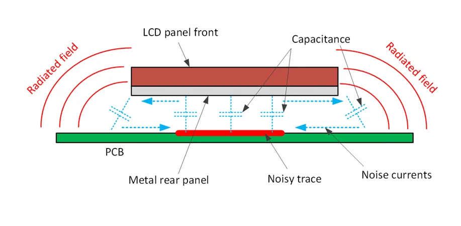
Another prevalent issue involves poor return current paths, where signals lack low-impedance references, enlarging loop areas that efficiently radiate energy. Differential-mode noise from power converters contrasts with common-mode noise on cables, each requiring distinct diagnostic approaches. In multilayer PCBs, split planes can force return currents to detour, amplifying magnetic fields. Resonances in PCB structures or enclosures further amplify emissions at specific frequencies. Electric engineers must recognize these symptoms, such as spurious peaks in spectrum analyzer readings, to initiate targeted troubleshooting.
Root Cause Analysis for EMI: Techniques and Best Practices
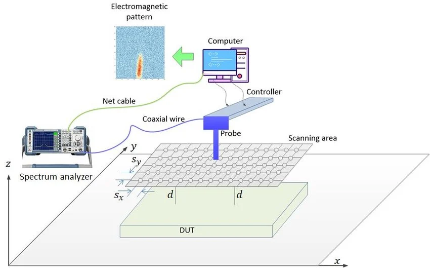
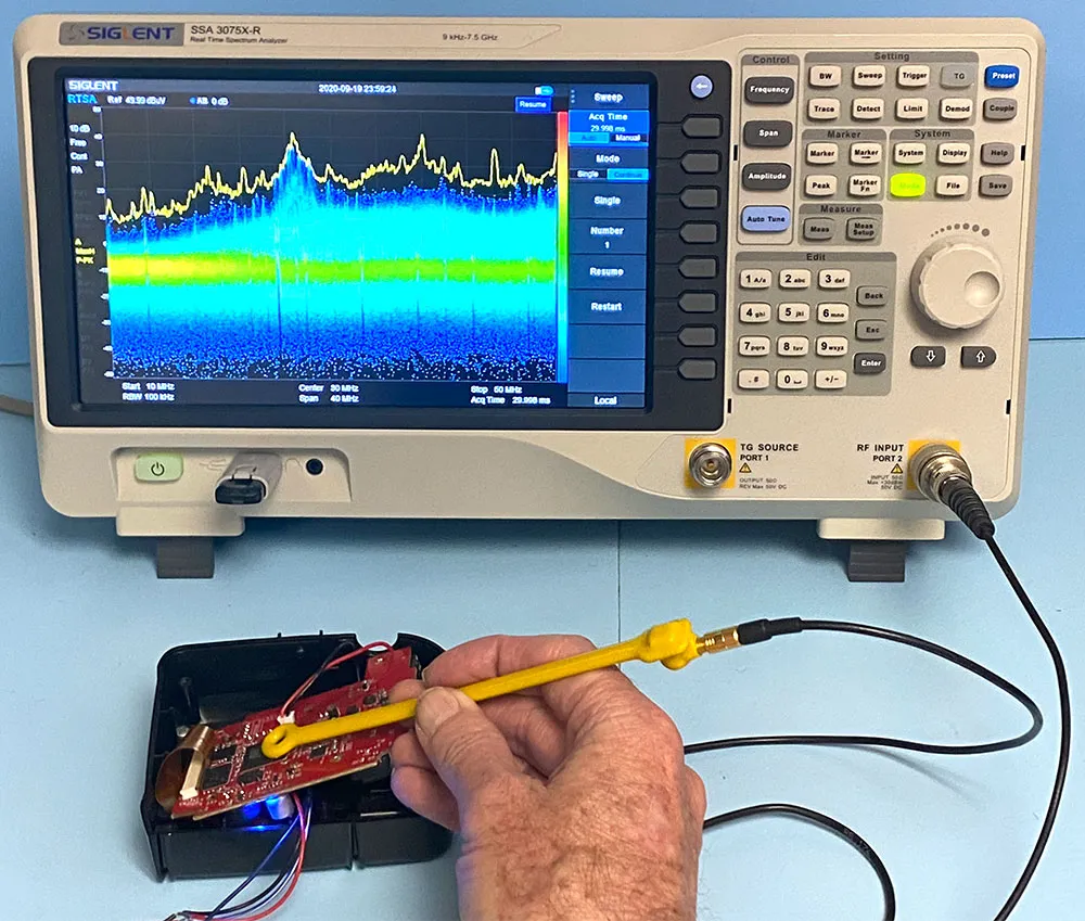
Effective root cause analysis EMI starts with spectrum analysis to pinpoint failure frequencies, correlating them to circuit elements like clock generators or data buses. Near-field scanning EMI emerges as a powerful, non-invasive method, using probes to map electric (E-field) and magnetic (H-field) emissions across the PCB surface. This technique reveals hotspots, such as noisy IC pins or trace segments, guiding precise interventions without full disassembly. Time-domain reflectometry complements by identifying impedance discontinuities that foster reflections and resonances. Systematic logging of test conditions, including enclosure status and cable configurations, ensures reproducibility during iterations.
In practice, isolate subsystems by powering sections sequentially to attribute emissions to specific modules. Current probe measurements on power rails quantify conducted noise sources. For complex boards, dipole modeling from near-field data predicts far-field radiation, aligning pre-compliance with chamber results. IPC-2221 guidelines emphasize design features that facilitate such analysis, like accessible test points and modular layouts. This structured root cause analysis EMI reduces guesswork, enabling fixes with minimal layout changes.
Handling EMI Testing Failures: A Step-by-Step Troubleshooting Guide
When EMI testing failures occur, begin by verifying test setup per relevant standards to rule out external variables. Reproduce the failure in a controlled bench environment using a spectrum analyzer and LISN for conducted tests. Apply near-field probes to localize the source, distinguishing between E-field dominant (capacitive) and H-field (inductive) radiators. Correlate peaks to schematics, noting harmonics or switching artifacts. Temporarily add mitigation like ferrites to confirm causality before permanent implementation.
Next, quantify margins against limits and prioritize fixes based on amplitude and reproducibility. Document iterations with before-and-after scans to track progress. Common pitfalls include overlooking enclosure interactions or loaded vs. unloaded conditions. This EMI troubleshooting guide stresses iterative verification, looping back to simulation if physical tweaks prove insufficient. Electric engineers benefit from checklists covering layout, decoupling, and shielding at each stage.
EMI Mitigation Strategies for Robust PCB Designs
Proven EMI mitigation strategies center on PCB layout optimization, starting with solid, unbroken ground and power planes to provide low-impedance return paths. Minimize loop areas by routing signals parallel to reference planes and using tight via fencing for shielding. Separate high-speed digital from analog sections with ground barriers to prevent noise spillover. Place decoupling capacitors close to IC power pins, selecting values for target frequencies based on self-resonance.
Filtering components like common-mode chokes and feed-through capacitors suppress conducted paths effectively. Guard traces or stitching vias along critical edges contain fields. IEC standards for EMC outline immunity levels that inform filter design choices. Enclosure shielding, achieved via conductive gaskets, addresses system-level radiation. Component selection favors low-EMI parts with spread-spectrum clocks to diffuse energy.
Advanced techniques include moats around noisy areas and balanced differential routing to cancel fields. Post-layout reviews per IPC-2221 verify clearances and impedance control. These layered EMI mitigation strategies, applied cumulatively, yield compliant designs with headroom for variations.
Real-World Troubleshooting Insights: A Hypothetical High-Speed Interface Case
Consider a high-speed serial interface board failing radiated emissions at 500 MHz harmonics. Initial near-field scanning pinpointed the transmitter IC as the dominant H-field source due to lengthy return loops. Root cause analysis revealed split planes forcing detours. Mitigation involved stitching vias to unify the plane and adding a ferrite bead on the clock line, reducing peaks by coupling noise to ground. Subsequent tests passed with margin, validating the approach. This scenario illustrates how targeted fixes resolve EMI testing failures efficiently.
Conclusion
Troubleshooting EMI demands a blend of diagnostic precision and design foresight, transforming common EMI problems into manageable engineering tasks. Key takeaways include leveraging near-field scanning for root cause analysis EMI, adhering to layout best practices, and verifying mitigations iteratively. Electric engineers armed with this EMI troubleshooting guide can preempt issues, streamline compliance, and deliver reliable products. Prioritizing EMI from schematic through assembly ensures success in an increasingly interconnected world. Implementing these EMI mitigation strategies not only resolves current challenges but builds resilience for future designs.
FAQs
Q1: What are the most common EMI problems in PCB designs, and how can they be spotted early?
A1: Common EMI problems include crosstalk, clock radiation, and ground bounce, often visible as unexpected peaks during pre-compliance scans. Spot them early via layout reviews for loop areas and simulations for impedance mismatches. Use EMI troubleshooting guide checklists to flag risks like adjacent high-speed traces. Proactive measures prevent escalation to full EMI testing failures.
Q2: How does near-field scanning EMI aid in root cause analysis?
A2: Near-field scanning EMI maps emission fields directly on the PCB, isolating sources like noisy traces or ICs without disassembly. Probes distinguish E and H fields, correlating to schematics for precise diagnosis. This technique accelerates root cause analysis EMI, enabling targeted fixes over broad redesigns. Combine with spectrum data for comprehensive insights.
Q3: What EMI mitigation strategies work best for high-speed boards?
A3: Effective EMI mitigation strategies feature solid reference planes, close decoupling, and filtering at noise sources. Route differentially and shield with vias to contain fields. Follow IPC-2221 for spacing rules. These steps reduce emissions systematically, ensuring pass in conducted and radiated tests.
Q4: Why do EMI testing failures occur, and how to avoid them?
A4: EMI testing failures stem from layout flaws, inadequate filtering, or cable resonances, amplified in loaded systems. Avoid by iterating pre-compliance with near-field tools and verifying per IEC EMC guidelines. Document margins and sensitivities for robust designs.
References
IPC-2221B — Generic Standard on Printed Board Design. IPC, 2009
IEC 61000-4-1 — Electromagnetic compatibility (EMC) - Part 4-1: Testing and measurement techniques - Overview of IEC 61000-4 series. IEC, 2006
IEC 61000-6-1 — Electromagnetic compatibility (EMC) - Part 6-1: Generic standards - Immunity for residential, commercial and light-industrial environments. IEC, 2016