Introduction
High-frequency PCB prototypes serve as critical validation tools for applications in telecommunications, radar systems, and high-speed data processing. These prototypes operate at frequencies typically above 1 GHz, where signal integrity becomes paramount due to wavelength effects comparable to board dimensions. Engineers often encounter issues like signal loss, impedance mismatch problems, EMI issues PCB faces, and crosstalk during initial testing phases. Troubleshooting these problems efficiently minimizes redesign cycles and accelerates time-to-market. Effective high-frequency PCB troubleshooting requires a blend of design knowledge, fabrication awareness, and precise measurement techniques. This article explores common pitfalls and practical remedies tailored for electrical engineers prototyping such boards.
Why High-Frequency PCB Prototyping Challenges Matter
In high-frequency environments, even minor deviations in PCB parameters can degrade performance significantly. Prototypes expose real-world discrepancies between simulations and fabricated boards, such as material inconsistencies or process variations. Addressing these early prevents costly iterations in production runs. Signal loss PCB experiences and impedance mismatch problems directly impact data rates and system reliability in 5G or automotive radar contexts. EMI issues PCB prototypes reveal can lead to compliance failures with regulatory emissions standards. Mastering crosstalk troubleshooting ensures cleaner signal transmission across dense layouts. For foundational principles before diving into troubleshooting, see our high-frequency PCB design guide for beginners.
Technical Principles Behind Signal Loss in High-Frequency PCBs
Signal loss in high-frequency PCBs arises primarily from conductor losses, dielectric losses, and radiation effects. Conductor losses dominate due to the skin effect, where current flows only in a thin outer layer of traces at high frequencies, increasing effective resistance. Dielectric losses stem from the material’s dissipation factor, converting signal energy into heat, especially in low-loss laminates under GHz ranges. Radiation losses occur when traces act as antennas, exacerbated by abrupt geometry changes or unshielded edges. These mechanisms compound in prototypes, where fabrication tolerances amplify losses beyond simulations. Understanding these principles guides targeted high-frequency PCB troubleshooting. Engineers often reference our comprehensive guide on minimizing signal loss in high-frequency PCBs for deeper material strategies.
Engineers measure total insertion loss using vector network analyzers, comparing S21 parameters against design goals. Prototype variations, like uneven plating thickness, intensify conductor losses. Dielectric constant fluctuations from moisture absorption further degrade performance. Radiation can be quantified via near-field probes during testing.
Causes and Detection of Impedance Mismatch Problems
Impedance mismatch problems in high-frequency PCB prototypes often result from trace width variations, dielectric thickness inconsistencies, or copper surface roughness. Fabrication processes introduce tolerances of plus or minus 10 percent in these parameters, shifting characteristic impedance from the targeted 50 ohms. In multilayer boards, via transitions and plane spacing further disrupt impedance continuity. Mismatches cause reflections, manifesting as ripple in frequency response or eye diagram closure in time-domain tests. Detection relies on time-domain reflectometry, where step response anomalies pinpoint discontinuity locations. These issues demand precise control during prototyping to maintain signal fidelity.
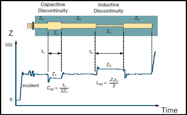
Reference planes must remain continuous to provide low-inductance return paths, yet prototype etching errors can create slots. Soldermask thickness variations subtly alter effective dielectric height. Engineers correlate impedance test results with cross-sections to validate root causes.
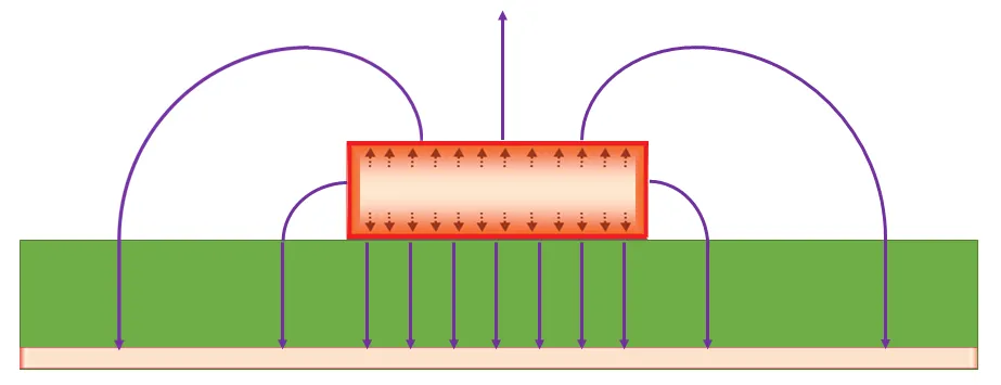
Mechanisms of EMI Issues in High-Frequency PCB Prototypes
EMI issues PCB prototypes exhibit stem from unintended radiation from high-speed traces and inadequate shielding. Common sources include clock lines, power planes with switching noise, and poor ground partitioning. Electromagnetic coupling occurs via electric fields between adjacent signals or magnetic fields through loop areas in return paths. At high frequencies, board edges radiate like slot antennas if not suppressed. Compliance testing reveals peaks violating limits, often traced to unterminated stubs or split planes. Isolating EMI sources requires systematic probing with spectrum analyzers.
Ground bounce amplifies emissions when multiple ICs share return paths, injecting noise into the power distribution network. Prototype assembly defects, such as lifted pads, exacerbate coupling paths. Fabricated prototypes highlight these when bench tests show spurious emissions.
Crosstalk Troubleshooting in Dense High-Frequency Layouts
Crosstalk troubleshooting addresses inductive and capacitive coupling between parallel traces in high-frequency PCB prototypes. Near-end crosstalk peaks when aggressor and victim traces switch simultaneously, injecting noise at the source. Far-end crosstalk diminishes with distance due to velocity differences but persists in tightly routed buses. Coupling strength scales inversely with trace spacing and directly with length and dielectric permittivity. Backward crosstalk from reflections complicates diagnosis. Engineers quantify it via mixed-mode S-parameters, isolating differential and common-mode effects.
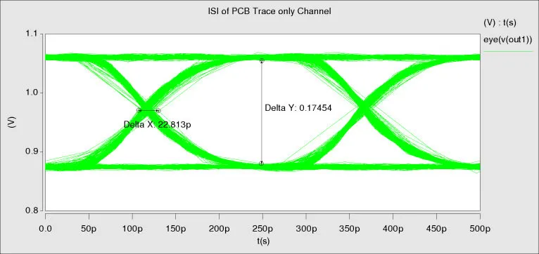
Prototype testing reveals layout sensitivities not captured in pre-layout simulations. Guard traces or stitching vias mitigate coupling but add complexity. Frequency-domain analysis distinguishes mutual inductance from capacitance dominance.
Optimal Material Selection and Stackup Design for Prototypes
Material selection and stackup design form the foundation for reliable high-frequency performance. Low-dielectric-constant (low-Dk) laminates minimize both propagation delay and loss, while low dissipation factors (Df) reduce heat generation. Symmetric stackups prevent warpage during lamination and reflow, maintaining impedance control across temperature cycles.
The table below compares common materials:
| Material | Dk (at 10 GHz) | Df (at 10 GHz) | Thermal Conductivity (W/m·K) | Moisture Absorption (%) | Typical Applications |
|---|---|---|---|---|---|
| FR-4 | 4.2–4.5 | 0.015–0.025 | 0.3 | 0.1–0.2 | Cost-sensitive, low-frequency |
| Rogers RO4003C | 3.38 | 0.0027 | 0.71 | 0.06 | RF/microwave, 5G antennas |
| RT/duroid 5880 | 2.20 | 0.0009 | 0.69 | 0.02 | High-performance radar, aerospace |
| Rogers RO4350B | 3.66 | 0.0037 | 0.69 | 0.05 | Cost-effective GHz prototypes |
Always consult the latest manufacturer datasheets, as values can vary slightly with frequency and resin content. For multilayer prototypes, aim for symmetric constructions with signal layers adjacent to solid reference planes and even copper distribution. This approach reduces warpage and supports tighter impedance tolerances.
Practical Solutions for High-Frequency PCB Troubleshooting
A structured approach to high-frequency PCB troubleshooting begins with visual inspection per IPC-A-600K acceptability criteria, checking for warpage, delamination, or plating voids. Electrical verification follows using flying probe testers for continuity and shorts before functional bring-up. For signal loss PCB concerns, de-embed fixtures calibrate measurements accurately. Impedance mismatch problems resolve through controlled-depth routing and material qualification matching design specs. EMI issues PCB prototypes face benefit from moat stitching and ferrite beads on power lines.
Crosstalk troubleshooting employs length matching and orthogonal routing orientations. Multilayer stacks incorporate dedicated ground planes adjacent to signal layers per IPC-6012E performance specs. Post-failure analysis involves dye-and-peel or cross-sectioning to correlate fab data with failures. Iterative prototyping refines PCB stackups for signal integrity, targeting loss tangents below 0.005.
- Signal Loss — Primary Cause: High tan delta; Quick Test Method: VNA S21 sweep; Mitigation Strategy: Low-loss dielectrics
- Impedance Mismatch — Primary Cause: Trace width variation; Quick Test Method: TDR; Mitigation Strategy: Tolerance-controlled fab
- EMI — Primary Cause: Poor grounding; Quick Test Method: Near-field probe; Mitigation Strategy: Full ground planes
- Crosstalk — Primary Cause: Close spacing; Quick Test Method: Eye diagram; Mitigation Strategy: Increased separation
Firmware tweaks, like slew rate control, complement hardware fixes during debug.
Advanced Testing and Validation Techniques
Advanced validation combines simulation with hardware measurement. Pre-fab, use tools such as Ansys HFSS or Keysight ADS for full-wave 3D electromagnetic simulation of the entire stackup and routing. Post-fab, TDR identifies impedance discontinuities with sub-millimeter resolution, while VNA S-parameter sweeps (up to 40 GHz) quantify insertion loss, return loss, and crosstalk.
A typical workflow:
- Extract parasitics from the fabricated board.
- Correlate simulation vs. measurement.
- Adjust models for actual copper roughness (Hammerstad or Groiss models).
- Re-spin only after confirming <5 % deviation.
These steps catch issues invisible to basic oscilloscopes and ensure prototypes meet stringent 5G or radar specifications.
Thermal Management and Manufacturing Considerations
High-frequency operation generates localized heat from dielectric and conductor losses, often requiring thermal vias, copper pours, or external heatsinks even in low-power prototypes. Account for coefficient of thermal expansion (CTE) mismatch between laminates and copper to prevent via cracking.
DFM guidelines include:
- Specifying copper roughness (VLP or RTF) for GHz traces.
- Allowing 10–15 % impedance margin for fab tolerances.
- Requesting impedance test coupons on every panel.
Early collaboration with the manufacturer on material availability and process windows prevents costly delays.
Advanced Troubleshooting Insights from Prototypes
Prototype teardowns often reveal subtle interactions, such as via resonance creating nulls in insertion loss curves. Engineers simulate post-fab geometries using extracted parasitics for correlation. Batch variations across prototype panels highlight process windows, guiding supplier specs. Combining thermal imaging with RF tests uncovers hotspots correlating to loss mechanisms. These insights refine design rules for volume production.
Conclusion
High-frequency PCB troubleshooting demands vigilance across signal loss PCB challenges, impedance mismatch problems, EMI issues PCB encounters, and crosstalk troubleshooting. By grasping underlying mechanisms and applying systematic tests aligned with standards like IPC-A-600K and IPC-6012E, engineers optimize prototypes effectively. Proactive measures, from material selection to layout rigor, ensure robust performance. Mastering these skills shortens development timelines and elevates design reliability.
FAQs
Q1: What are the main causes of signal loss PCB in high-frequency prototypes?
A1: Signal loss PCB primarily results from skin effect in conductors, dielectric dissipation, and radiation from traces. Prototype fabrication introduces surface roughness and thickness variations that worsen losses. Engineers mitigate this by selecting low-loss materials and verifying with VNA measurements. Consistent plating processes maintain performance margins.
Q2: How do you identify impedance mismatch problems during high-frequency PCB troubleshooting?
A2: Impedance mismatch problems manifest as reflections in TDR waveforms or S11 peaks on VNAs. Prototype tolerances in etch and laminate thickness cause shifts from nominal values. Cross-section analysis confirms root causes. Adjust stackups and routing for continuity in revisions.
Q3: What steps resolve EMI issues PCB prototypes commonly face?
A3: EMI issues PCB prototypes exhibit arise from noisy traces and incomplete shielding. Implement solid ground planes, via fences, and decoupling capacitors near sources. Spectrum analyzer scans localize emitters. Partition sensitive analog sections from digital.
Q4: Why is crosstalk troubleshooting critical in high-frequency designs?
A4: Crosstalk troubleshooting prevents noise injection between traces, degrading eye openings at GHz speeds. Measure with multi-channel scopes and adjust spacing or add shields. Prototype testing validates guard traces effectiveness.
References
IPC-A-600K — Acceptability of Printed Boards. IPC, 2020
IPC-6012E — Qualification and Performance Specification for Rigid Printed Boards. IPC, 2017


