Introduction
Copper weight plays a critical role in PCB stack-up design, directly influencing electrical performance, thermal management, and mechanical reliability. For electric engineers, selecting the appropriate PCB copper weight ensures that boards can handle required current loads without excessive heating or voltage drops. This guide explores the fundamentals of copper thickness PCB, its impact on current carrying capacity PCB, and considerations for PCB power planes and heavy copper PCB applications. Understanding these elements helps optimize multilayer stack-ups for high-reliability designs in power electronics, automotive systems, and telecommunications. By aligning copper weight with stack-up requirements, engineers can balance cost, manufacturability, and performance effectively.
What Is PCB Copper Weight?
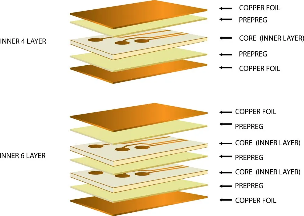
PCB copper weight refers to the mass of copper per unit area on the foil, typically measured in ounces per square foot (oz/ft2). Common values include 0.5 oz/ft2, 1 oz/ft2, 2 oz/ft2, and higher for specialized applications. This metric directly correlates to copper thickness PCB, where 1 oz/ft2 equates to approximately 35 micrometers of pure copper thickness. In a PCB stack-up, each signal, ground, or power layer specifies its copper weight, which affects the overall board thickness and interlayer spacing. Manufacturers electrodeposit copper onto laminate cores, building up the specified weight during the panelization process. Engineers must specify copper weight uniformly or vary it across layers based on functional needs.
Why Copper Weight Matters in PCB Stack-Up Design
In multilayer PCBs, copper weight determines the current carrying capacity PCB, which is essential for preventing thermal runaway in high-power circuits. Thicker copper reduces resistance, allowing wider traces or planes to carry more amperage with minimal temperature rise. For PCB power planes, heavier copper weights improve voltage distribution and reduce inductance in dense stack-ups. Mechanical stability also benefits, as thicker copper resists warpage during thermal cycling and soldering processes. Poor copper weight selection can lead to delamination or via failures under stress, compromising long-term reliability. Electric engineers prioritize this parameter early in stack-up planning to meet system-level performance targets.
Copper Thickness vs Current Carrying Capacity in PCBs
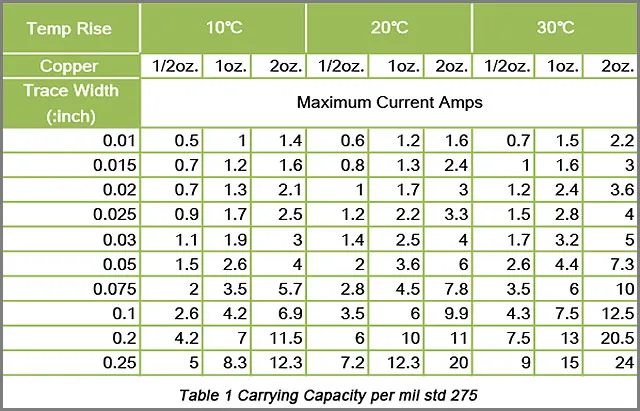
Copper thickness PCB directly governs current carrying capacity PCB through Ohm's law and thermal dissipation principles. Thicker copper lowers trace resistance, enabling higher currents before reaching allowable temperature rises, typically 10 to 20 degrees Celsius above ambient. Factors like trace width, ambient temperature, and airflow further modulate capacity, but copper weight sets the baseline. In stack-ups, internal layers with heavier copper handle power routing efficiently, minimizing voltage drops across the board. Engineers calculate capacities using empirical models that account for copper's thermal conductivity of about 400 W/m·K. IPC-2152 provides guidelines for these calculations, emphasizing cross-sectional area over simplistic width-based rules.
Narrow traces on thin copper may suffice for signal integrity, but power traces demand heavier weights to avoid hotspots. For example, a 1 oz/ft2 trace might limit current to levels unsuitable for motor drives, necessitating upgrades to 2 oz/ft2 or more. Surrounding dielectric materials influence heat spreading, making stack-up materials a complementary consideration. Testing validates designs, ensuring real-world performance aligns with simulations.
Suggested Reading: Choosing PCB Copper Weight: 1oz vs. 2oz for Optimal Performance
Optimizing Copper Weight for PCB Power Planes
PCB power planes rely on solid copper fills to deliver low-impedance paths for DC and high-frequency currents. Heavier copper weights in power planes enhance current carrying capacity PCB by increasing cross-sectional area, reducing plane resistance to milliohms. In dense stack-ups, planes sandwich between dielectrics, where 1 oz/ft2 often suffices for low-power designs, but 2 oz/ft2 or more supports high-current applications like server motherboards. Plane splits and stitching vias manage return paths, with copper thickness mitigating skin effect losses at MHz frequencies. Engineers balance plane weight with core thickness to control impedance and maintain signal integrity on adjacent layers. Excessive weight increases board cost and weight, so targeted thickening via partial plating is common.
Heavy Copper PCB Applications & Manufacturing
Heavy copper PCB designs exceed 3 oz/ft2, up to 20 oz/ft2 in extreme cases, for applications demanding exceptional current carrying capacity PCB, such as inverters and welding equipment. These boards feature differentially etched traces where wide power paths contrast with fine-pitch signals, requiring precise stack-up control. Manufacturing challenges include etching undercuts in thick copper, addressed through tented vias and sequential lamination per IPC-6012 standards. Thermal expansion mismatches between heavy copper and thinner layers can induce stress, necessitating robust prepregs with high Tg values. Electric engineers specify heavy copper strategically, often combining it with embedded capacitors in the stack-up for integrated power delivery. Post-fabrication, X-ray inspection verifies plating uniformity.
Key Factors for Copper Weight Selection in Stack-Ups
Several interrelated factors guide copper weight choices in PCB stack-ups. Electrical requirements, including peak currents and duty cycles, dictate minimum thicknesses for traces and planes. Thermal simulations predict hotspots, ensuring compliance with IPC-A-600 acceptability criteria for surface finishes and plating. Mechanical demands, like vibration resistance in aerospace, favor heavier copper for structural integrity. Cost implications rise nonlinearly with weight, as heavier foils demand longer plating times and specialized presses. Engineers iterate stack-ups using layer tables that list copper weight, dielectric thickness, and impedance targets.
- Top Signal — Copper Weight: 1 oz/ft2 — Function: Components/Signals — Dielectric Thickness: -
- Power Plane — Copper Weight: 2 oz/ft2 — Function: VCC Distribution — Dielectric Thickness: 5 mil
- Ground Plane — Copper Weight: 1 oz/ft2 — Function: Return Path — Dielectric Thickness: 5 mil
- Inner Signal — Copper Weight: 1 oz/ft2 — Function: Routing — Dielectric Thickness: 5 mil
- Bottom Signal — Copper Weight: 1 oz/ft2 — Function: Components — Dielectric Thickness: -
This sample stack-up illustrates balanced weights for a mid-power design.
Best Practices for Specifying Copper Weight
Start with system-level current analysis to baseline copper thickness PCB needs across the stack-up. Use conservative margins for derating, applying 70-80% of calculated current carrying capacity PCB under worst-case conditions. Collaborate with fabricators early to confirm reverse-pulse plating capabilities for heavy copper PCB. Vary weights judiciously: thin outer layers for fine-pitch components, thicker internals for power. Simulate electromagnetic fields to verify plane interactions, adjusting weights if crosstalk exceeds limits. Document stack-up drawings with copper weights, tolerances, and IPC references for unambiguous quoting.
Validate prototypes through thermal cycling and current stress tests, correlating to IPC-6012 performance specs. Partial heavy copper, where only power regions thicken, optimizes cost without compromising signals. Monitor via current limits separately, as plating thickness affects barrel reliability.
Common Copper Weight Challenges & Solutions
Uneven plating can degrade current carrying capacity PCB, manifesting as hotspots during high-load operation. Engineers troubleshoot by reviewing panel utilization and current density logs from fabrication. Warpage in heavy copper PCB stack-ups arises from CTE mismatches; countermeasures include symmetric layering and constrained lamination. Impedance deviations from thick planes require prepreg adjustments for consistent dielectric spacing. Field failures often trace to underrated copper weights, underscoring the need for margin in designs. Post-mortem analysis refines future stack-ups.
Conclusion
Mastering PCB copper weight in stack-ups empowers electric engineers to deliver robust, efficient boards tailored to demanding applications. From standard 1 oz/ft2 signals to heavy copper PCB power planes, thoughtful selection enhances current carrying capacity PCB while upholding reliability. Adhering to best practices and standards ensures manufacturability without compromising performance. As designs evolve toward higher powers, precise copper thickness PCB control remains foundational. Integrate these principles into your workflow for superior outcomes.
FAQs
Q1: What is the standard copper weight used in most PCB stack-ups?
A1: In typical multilayer PCB stack-ups, 1 oz/ft2 (35 μm) serves as the baseline for signal and ground layers due to its balance of cost, etch precision, and adequate current carrying capacity PCB. Power planes may upgrade to 2 oz/ft2 for enhanced distribution. Fabricators confirm feasibility based on design rules, ensuring compliance with IPC guidelines. This weight supports most commercial electronics without excessive thermal rise.
Q2: How does copper thickness PCB affect current carrying capacity?
A2: Copper thickness PCB determines cross-sectional area, inversely proportional to resistance and thus directly boosting current carrying capacity PCB. Doubling from 1 oz/ft2 to 2 oz/ft2 roughly doubles capacity for a given width and temperature rise. Engineers factor in ambient conditions and trace geometry per IPC-2152 models. This relationship guides stack-up optimization for power-intensive circuits.
Q3: When should you specify heavy copper PCB?
A3: Opt for heavy copper PCB exceeding 3 oz/ft2 when designs exceed 10-20A per trace or require compact power planes with low losses. Applications like power supplies and EVs benefit from its superior current carrying capacity PCB. Manufacturing demands sequential processes for etch control. Balance with cost by localizing heavy areas.
Q4: What role do PCB power planes play in stack-up copper weight?
A4: PCB power planes use heavier copper weights to minimize voltage drops and inductance in multilayer stack-ups. They provide uniform distribution for ICs, with thickness tailored to total current load. Ground planes pair symmetrically for EMI control. Proper weighting per IPC standards prevents resonance issues.
References
IPC-2152B — Standard for Determining Current Carrying Capacity in Printed Board Design. IPC, 2023
IPC-6012E — Qualification and Performance Specification for Rigid Printed Boards. IPC, 2017
IPC-A-600K — Acceptability of Printed Boards. IPC, 2020


