Introduction
The rollout of 5G networks has transformed telecommunications infrastructure, demanding printed circuit boards that handle frequencies from sub-6 GHz up to millimeter-wave bands beyond 20 GHz. High-frequency PCB laminates play a critical role in maintaining signal integrity amid these elevated speeds and data rates. Engineers must select 5G PCB materials that minimize losses and ensure stable performance under demanding conditions. This article explores the key properties of low loss PCB material and dielectric constant PCB considerations, providing structured guidance for optimal laminate choices. By focusing on engineering principles, it equips electric engineers with actionable insights for reliable 5G designs.
Why High-Frequency PCB Laminates Matter for 5G Networks
5G applications push PCB designs into regimes where standard materials like FR-4 introduce unacceptable signal degradation. High-frequency signals experience greater attenuation and phase shifts, leading to reduced data throughput and increased error rates. Low loss PCB material becomes essential to preserve signal power over long traces and complex routing. Dielectric constant PCB stability ensures predictable impedance control, vital for matching antennas and transceivers in base stations and user equipment. Without proper laminate selection, issues like crosstalk and reflections compromise overall network performance. Engineers prioritize these materials to meet the stringent requirements of modern wireless systems.
The shift to 5G also amplifies thermal and mechanical stresses from power amplifiers and dense component integration. Laminates must withstand repeated thermal cycling without delamination or warpage. Industry standards such as IPC-4101 define qualification criteria for base materials, ensuring consistency in electrical and physical properties. This foundation supports scalable manufacturing for 5G deployments. Ultimately, selecting the right high-frequency PCB laminates directly impacts reliability and efficiency in real-world environments.
Key Technical Properties of 5G PCB Materials
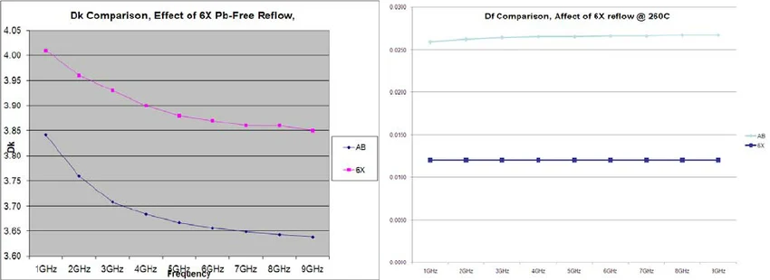
The dielectric constant, or Dk, determines signal propagation speed through the laminate, calculated as velocity equals the speed of light divided by the square root of Dk. Lower Dk values, typically in the range of 2.2 to 3.5 for high-performance materials at 10 GHz, reduce delay and enable tighter impedance control. Variations in Dk across frequency or temperature can cause mismatches, distorting signals in 5G mmWave paths. Engineers evaluate Dk stability using test methods outlined in standards like IPC-TM-650, focusing on consistency from 1 MHz to beyond 10 GHz.
Dissipation factor, or Df (loss tangent), quantifies energy loss as heat in the dielectric, directly affecting insertion loss. For 5G PCB materials, Df values below 0.005 at 10 GHz minimize attenuation, especially critical for longer traces in base stations. High Df exacerbates skin effect losses at microwave frequencies, degrading return loss and eye diagrams. Low loss PCB material with controlled Df ensures high data rates without excessive power consumption. Material isotropy further enhances performance by providing uniform properties in all directions.
Thermal properties influence long-term reliability in 5G environments. The coefficient of thermal expansion (CTE) must match copper foil, typically around 17 ppm/°C in X/Y directions, to prevent stress during soldering or operation. Low moisture absorption preserves electrical stability, as water increases effective Dk and Df. Glass transition temperature (Tg) indicates rigidity under heat, with higher values resisting deformation. Mechanical strength, including peel strength and dimensional stability, supports high-density interconnects.
Criteria for Selecting Laminates in High-Frequency 5G Designs
Engineers begin laminate selection by defining frequency bands: sub-6 GHz tolerates moderately low loss materials, while mmWave demands ultra-low Df options like PTFE-based composites. Dielectric constant PCB choices prioritize stability over absolute value, with tolerances under ±0.05 for precise modeling. Simulate stackups to verify characteristic impedance, using formulas like the microstrip approximation from IPC-2141. Hybrid constructions pair high-frequency cores with cost-effective inner layers for balanced performance.
Consider thermal conductivity for heat dissipation from 5G power components, favoring materials above 0.5 W/m-K where possible. IPC-4103 specifies requirements for high-speed laminates, emphasizing low Df variation and isotropic behavior. Evaluate moisture sensitivity through preconditioning tests to simulate field conditions. Mechanical robustness counters warpage in multilayer builds, guided by CTE matching and symmetrical stackups.
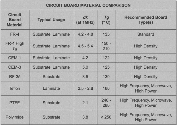
- Property: Dk at 10 GHz — Standard Laminate (e.g., FR-4): 4.2–4.7; High-Frequency Laminate: 2.2–3.5
- Property: Df at 10 GHz — Standard Laminate: 0.015–0.025; High-Frequency Laminate: 0.001–0.005
- Property: Typical Tg (°C) — Standard Laminate: 130–170; High-Frequency Laminate: 200+
- Property: Moisture Absorption (%) — Standard Laminate: 0.1–0.2; High-Frequency Laminate: <0.1
- Property: CTE X/Y (ppm/°C) — Standard Laminate: 15–20; High-Frequency Laminate: 10–20
This comparison highlights trade-offs, with high-frequency PCB laminates offering superior electrical traits at higher cost.
Fabrication compatibility influences choices, as some low loss materials require special drilling or plating processes. Qualification per IPC-6012 ensures performance under qualification and performance specs for rigid boards. Prototype testing with time-domain reflectometry verifies impedance and losses.
Best Practices for Implementing High-Frequency Laminates in 5G PCBs
Start with application mapping: use ceramic-filled epoxies for sub-6 GHz and pure PTFE for mmWave to optimize cost-performance. Maintain outer-layer routing for RF signals to leverage lower loss paths. Employ blind or buried vias to minimize stubs, back-drilling where necessary above 10 GHz. Ground plane stitching with vias spaced less than half-wavelength prevents radiation.
Control stackup symmetry to avoid warpage, targeting dielectric thicknesses of 0.127–0.254 mm for mmWave. Select copper types like low-profile reverse-treated foil to reduce surface roughness losses. Environmental screening per IPC standards confirms reliability across -55°C to 125°C. Document specifications clearly, referencing slash sheets from IPC-4101 for reproducibility.
Integrate thermal vias and heat sinks early, as 5G amplifiers generate localized hotspots. Field trials validate performance before volume production.
Troubleshooting Common Issues in 5G Laminate Selection
Signal attenuation often stems from inadequate Df control; audit materials against frequency needs. Impedance drifts arise from Dk variations; specify tight tolerances and measure post-fabrication. Warpage in assemblies points to CTE mismatch; opt for matched laminates and symmetric builds. Delamination under humidity signals high moisture absorption; precondition per JEDEC J-STD-020 standards.
Conclusion
Selecting 5G PCB materials hinges on balancing low Dk, minimal Df, and robust thermal-mechanical properties for high-frequency performance. High-frequency PCB laminates enable the speed and reliability 5G demands, from base stations to handsets. Adhering to standards like IPC-4101 and IPC-4103 ensures qualified, repeatable results. Engineers achieve optimal designs by simulating, prototyping, and testing rigorously. This approach future-proofs networks against evolving wireless challenges.
FAQs
Q1: What are the primary properties to consider in 5G PCB materials?
A1: For electric engineers, prioritize low dielectric constant PCB values (Dk 2.2–3.5) and dissipation factor (Df <0.005 at 10 GHz) to minimize signal delay and loss. Thermal stability, low CTE, and moisture resistance support reliability in high-power 5G environments. Follow IPC-4103 for high-speed laminate specs to ensure consistency.
Q2: How do high-frequency PCB laminates differ from standard materials for 5G?
A2: High-frequency PCB laminates feature lower loss PCB material traits, like Df below 0.005 versus about 0.02 for FR-4, reducing attenuation at mmWave frequencies. They offer better Dk stability across temperatures, aiding impedance control. Mechanical enhancements prevent warpage in dense 5G stackups.
Q3: Why is dielectric constant critical in Rogers PCB 5G applications?
A3: Dielectric constant PCB directly affects propagation speed and impedance in Rogers PCB 5G designs, where stable low Dk prevents reflections. Variations amplify phase errors in phased arrays. Select materials with minimal frequency-dependent changes for optimal antenna performance.
Q4: What standards guide low loss PCB material qualification?
A4: IPC-4101 and IPC-6012 provide qualification frameworks for electrical, thermal, and mechanical properties. IPC-4103 targets high-frequency needs with Df and Dk controls. These ensure 5G PCB materials meet performance under stress.
References
IPC-4101E — Specification for Base Materials for Rigid and Multilayer Printed Boards. IPC.
IPC-4103 — Specification for High Speed/High Frequency Laminate and Prepreg Materials. IPC.
IPC-6012E — Qualification and Performance Specification for Rigid Printed Boards. IPC, 2017.
JEDEC J-STD-020E — Moisture/Reflow Sensitivity Classification. JEDEC, 2014.


