Introduction
5G telecommunication base stations operate at millimeter wave frequencies, typically from 24 GHz to 100 GHz, to deliver ultra-high data rates and low latency. These frequencies enable massive MIMO configurations and beamforming essential for handling dense user traffic in urban environments. However, 5G PCB design for base stations faces unique hurdles due to the short wavelengths that amplify losses and sensitivities in printed circuit boards. Engineers must address signal integrity, material selection, and integration of antenna arrays to ensure reliable performance. This article explores the core challenges in millimeter wave PCB design and provides structured solutions grounded in engineering principles. Understanding these aspects is critical for optimizing base station efficiency and meeting deployment demands.
Why Millimeter Wave PCB Design Matters for 5G Base Stations
Millimeter wave PCB refers to boards engineered for signals above 30 GHz, where traditional FR-4 materials fail due to excessive attenuation. In 5G base stations, these PCBs support active antenna units that integrate RF transceivers, power amplifiers, and phased arrays directly on the board. High-frequency PCB design becomes pivotal as it directly impacts throughput, coverage, and energy efficiency in networks serving billions of connected devices. Without precise control over transmission paths, signal loss in PCB traces can degrade beamforming accuracy and increase error rates. Moreover, base stations often require multi-layer stackups to route digital control signals alongside RF paths, complicating the layout. Prioritizing millimeter wave PCB expertise ensures compliance with performance targets and scalability for future 6G evolutions.
Key Challenges in High-Frequency PCB Design for 5G
At millimeter wave frequencies, signal propagation encounters severe attenuation from conductor, dielectric, and radiation losses. Conductor losses dominate due to the skin effect, where current flows only on the copper surface, making surface roughness a critical factor. Dielectric losses arise from the material's dissipation factor, which converts signal energy to heat, especially over longer traces. Radiation losses occur when discontinuities like bends or vias leak energy into the substrate. These combined effects limit trace lengths to centimeters, demanding compact layouts in base station PCBs. Engineers must model these interactions meticulously to predict real-world performance.
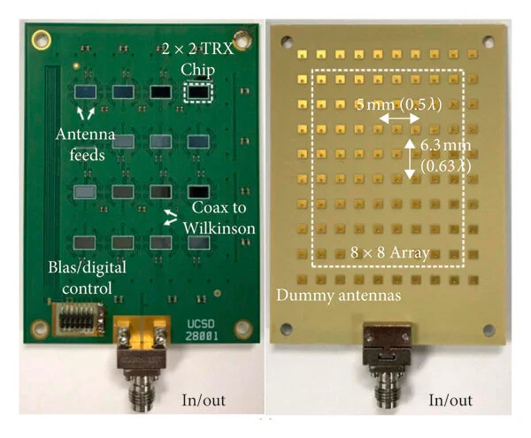
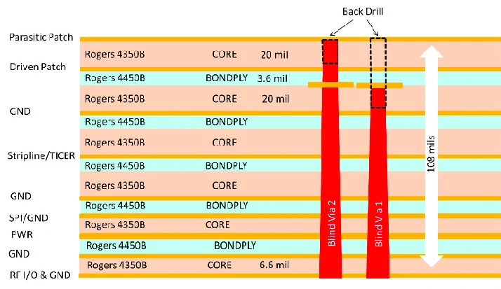
Impedance control poses another hurdle in 5G PCB design, as tolerances below 5% are often required for 50-ohm lines. Variations in dielectric thickness or copper width, even microns, shift characteristic impedance and cause reflections. In multi-layer boards, asymmetric stackups lead to warpage under thermal stress, misaligning vias and antennas. Antenna PCB design integrates patch or slot elements directly on the board, but coupling between elements in dense arrays introduces mutual interference. Thermal management challenges intensify with high-power amplifiers generating heat densities exceeding 10 W/cm2, risking delamination or performance drift. Fabrication tolerances tighten to sub-micron levels, straining standard processes.
Signal loss in PCB escalates exponentially with frequency, following the relation α_total = α_c + α_d + α_r, where each term grows nonlinearly. For instance, at 28 GHz, a 10 cm trace might incur 3-5 dB loss, halving signal power without mitigation. Vias introduce inductive stubs that resonate at mmWave, reflecting up to 20% of power if not optimized. Crosstalk between parallel traces rises due to stronger electromagnetic coupling at short wavelengths. Power integrity issues emerge from simultaneous switching of digital lines feeding beamforming ICs, creating noise that couples into RF paths. These challenges necessitate a holistic approach from schematic to fabrication.
Engineering Mechanisms Behind mmWave PCB Challenges
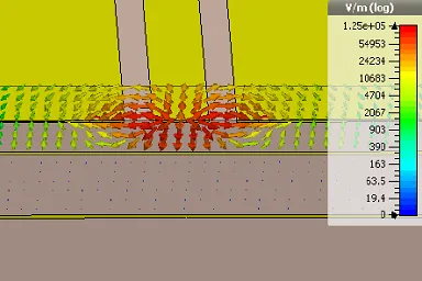
The skin depth δ at frequency f is given by δ = √(2/(ω μ σ)), shrinking to under 1 μm at 60 GHz, confining current to rough copper peaks and valleys. This roughness, quantified by RMS values, increases effective resistivity by 20-50% compared to smooth foil. Dielectric constant Dk and loss tangent Df determine propagation constant, with Df > 0.005 causing unacceptable attenuation in base station links. Substrate modes propagate unwanted energy parallel to traces, especially in thick dielectrics, degrading isolation. In antenna PCB design, surface waves from feed lines distort radiation patterns, reducing gain by several dB. Thermal expansion mismatch between layers, governed by CTE coefficients, induces stress during soldering per IPC-6012E qualification.
Per IPC-2221 guidelines, trace width w for microstrip impedance Z0 ≈ 50 Ω is w/h ≈ (8/e^{A} + w/4h)/(e^{A}-2), where A relates to effective ε_r, demanding precise etch control. At mmWave, embedded transmission lines like grounded coplanar waveguide (GCPW) minimize losses by supporting quasi-TEM modes with better confinement. However, transitions from microstrip to GCPW create modal discontinuities, requiring tapered sections. Via fences or stitching grounds suppress slotline modes excited at junctions. Mechanical stability under vibration in outdoor base stations requires rigid-flex hybrids, but flex regions introduce higher losses. These mechanisms underscore the need for simulation-driven design.
Practical Solutions and Best Practices for 5G PCB Design
Select laminates with low Df (<0.002) and stable Dk (2.5-3.5) across temperature and humidity to combat dielectric losses. Use low-profile copper foils with RMS roughness <0.5 μm to reduce conductor losses by up to 30%. Symmetric stackups with thin cores (50-100 μm) prevent warpage and support tight coupling. For signal loss in PCB, limit trace lengths and employ serpentine routing with mitered bends at 45 degrees to minimize reflections. Backdrill vias to stubs < λ/20 and use filled vias for lower inductance in high-power paths.
In high-frequency PCB design, prioritize stripline over microstrip for shielded propagation, embedding signals between ground planes spaced 0.1-0.2 mm. Ground vias spaced λ/10 around traces form effective shields against crosstalk. Antenna PCB design benefits from cavity-backed patches etched on the top layer, with feed networks routed on inner layers to avoid interference. Implement beamforming calibration ports with matched terminations to maintain phase accuracy. Thermal vias under amplifiers, combined with metal pours, dissipate heat while preserving RF isolation. Adhere to IPC-A-600K acceptability criteria for surface finishes like ENIG to ensure low-loss solder joints.
Advanced techniques include suspended microstrip with air gaps for ultra-low loss, achieved via selective etching. Hybrid integration mounts GaN amplifiers off-board with minimal interconnects. Fabrication partners should validate designs via TRL calibration measurements up to 110 GHz. Post-fabrication, perform S-parameter sweeps to verify insertion loss <1 dB/inch. These practices, when combined, yield robust millimeter wave PCBs for base stations.
Troubleshooting Common Issues in Millimeter Wave PCBs
Unexpected resonances often stem from unbackdrilled vias; inspect via stubs via time-domain reflectometry. High insertion loss points to copper roughness; switch to reverse-treated foil. Antenna pattern distortion indicates surface wave excitation; add guard rings or absorbers. Thermal runaway in arrays requires enhanced copper planes and CTE-matched materials. Crosstalk spikes suggest inadequate ground stitching; densify vias to <λ/20 spacing. Systematic DFT insertion aids field diagnostics.
Conclusion
5G telecommunication base station PCB design at millimeter wave frequencies demands overcoming signal loss, impedance variations, and integration complexities through precise materials and layouts. Low-loss stackups, optimized vias, and shielded lines form the backbone of effective solutions. Adhering to standards like IPC-6012E and IPC-A-600K ensures reliability. Engineers equipped with these strategies can deliver high-performance boards that power next-generation networks. Future advancements will further refine these approaches for even higher frequencies.
FAQs
Q1: What are the primary causes of signal loss in PCB for 5G mmWave applications?
A1: Signal loss in PCB arises from conductor effects like skin depth reduction and copper roughness, dielectric dissipation, and radiation at discontinuities. At 28 GHz and above, these losses accumulate rapidly, often exceeding 2 dB per cm without mitigation. Low-profile copper and Df <0.002 materials reduce attenuation effectively. Proper via design and shielding further minimize leakage.
Q2: How does high-frequency PCB design differ for millimeter wave base stations?
A2: High-frequency PCB design for mmWave emphasizes thin dielectrics, symmetric stackups, and transmission lines like GCPW to control impedance and modes. Antenna integration requires array spacing at λ/2 for beamforming. Fabrication tolerances tighten to microns, unlike lower frequencies. This ensures low loss and phase stability critical for 5G performance.
Q3: What solutions mitigate challenges in antenna PCB design for 5G?
A3: Antenna PCB design solutions include cavity-backed elements to suppress surface waves and dense ground stitching for isolation. Phased array feeds use Wilkinson dividers on inner layers. Material selection with stable Dk prevents pattern shifts. Simulation verifies gain and sidelobes before fabrication.
Q4: Why is impedance control vital in 5G PCB design?
A4: Impedance control prevents reflections that degrade signal integrity in millimeter wave paths. Tolerances under 5% are essential for VSWR <1.2 across bands. Stackup symmetry and etch precision achieve this. Variations cause beam squint in arrays, impacting base station coverage.
References
IPC-6012E — Qualification and Performance Specification for Rigid Printed Boards. IPC, 2017
IPC-A-600K — Acceptability of Printed Boards. IPC, 2020
IPC-2221 — Generic Standard on Printed Board Design. IPC, 2012


