Introduction
Marine navigation systems rely on high-frequency signals for critical functions like radar detection, GPS positioning, and communication links. These systems operate in harsh environments exposed to saltwater corrosion, mechanical vibrations, and temperature fluctuations, making PCB design a pivotal factor in overall reliability. High-frequency PCB layout techniques ensure that signals maintain integrity from transmitter to receiver, preventing data corruption that could lead to navigational errors. Engineers must address challenges such as electromagnetic interference and dielectric losses unique to marine applications. This article explores advanced strategies for impedance control, signal routing, and antenna integration tailored to these demanding conditions. By focusing on proven engineering principles, designers can achieve robust performance in signal integrity marine PCBs.
The Importance of High-Frequency PCB Layout in Marine Navigation Systems
High-frequency PCB layout directly impacts the accuracy and safety of marine navigation by preserving signal quality over gigahertz ranges. In systems like radar arrays or satellite receivers, even minor layout flaws can amplify reflections or crosstalk, degrading resolution and range. Marine environments exacerbate these issues through humidity-induced absorption and vibration-induced micro-cracks in traces. Proper layout minimizes these risks, ensuring compliance with performance demands in compact enclosures. For electric engineers, mastering these techniques translates to fewer field failures and extended system lifespans. Ultimately, effective high-frequency PCB layout supports seamless integration of RF components with digital processing units.
Key Technical Principles for High-Frequency Signal Propagation
At high frequencies, signals behave as transmission lines rather than simple wires, governed by characteristic impedance defined by trace geometry and substrate properties. Impedance mismatches cause reflections, quantified by the reflection coefficient, which distorts waveforms and reduces eye diagram margins. Dielectric materials with low loss tangents are essential to curb attenuation, while conductor surface roughness affects skin effect losses. Ground plane proximity influences return path inductance, critical for loop impedance minimization. Engineers must model these interactions using field solvers to predict behavior before fabrication. Understanding these principles forms the foundation for impedance control PCB designs in marine systems.
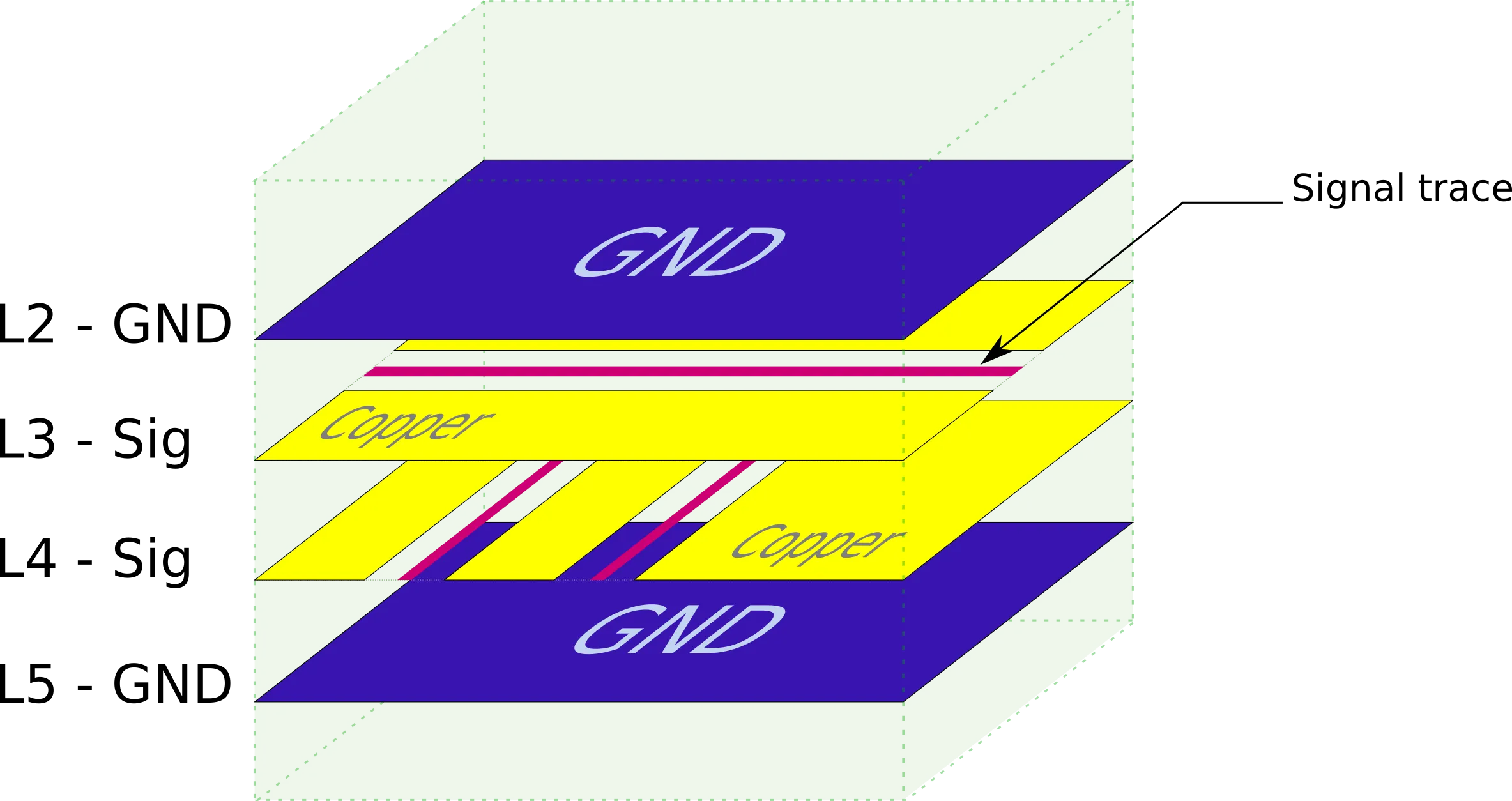
Crosstalk arises from mutual inductance and capacitance between adjacent traces, worsening at higher frequencies due to faster rise times. Differential signaling pairs require symmetric routing to balance common-mode rejection. Via transitions introduce discontinuities, acting as stubs that resonate at quarter-wavelength frequencies. Power plane splitting must avoid signal crossings to prevent ground bounce. These mechanisms demand layered stackups with dedicated planes for signals and returns. Adhering to IPC-2141A guidelines ensures controlled impedance across the board.
Advanced Layout Techniques for Impedance Control and Signal Integrity
Impedance control PCB strategies begin with stackup definition, alternating signal layers with ground or power planes to achieve 50-ohm single-ended or 100-ohm differential targets. Trace width and spacing are calculated based on dielectric thickness and effective permittivity, verified through time-domain reflectometry post-fabrication. Microvia and blind via usage reduces stub lengths in multilayer boards, preserving high-frequency response. Routing high-speed signals on inner layers shields them from external noise, vital for signal integrity marine PCB applications. Length-matched serpentine patterns equalize propagation delays in clock distribution networks. These techniques collectively mitigate reflections and maintain bit error rates below acceptable thresholds.
Grounding schemes employ stitched vias around critical sections to form low-impedance return paths, reducing radiated emissions. Partitioned planes with stitching capacitors bridge splits, avoiding resonance modes. Component placement prioritizes RF chains, grouping amplifiers and mixers to shorten interconnects. Decoupling capacitors near IC pins supply instantaneous currents, stabilizing voltage rails. Simulation validates these layouts by analyzing S-parameters for insertion loss and return loss. In marine navigation, such precision prevents intermittent failures under dynamic loads.
Related Reading: Optimizing Power Distribution in Marine Navigation PCBs: A Comprehensive Guide
Microstrip Antenna Design Considerations for Marine Applications
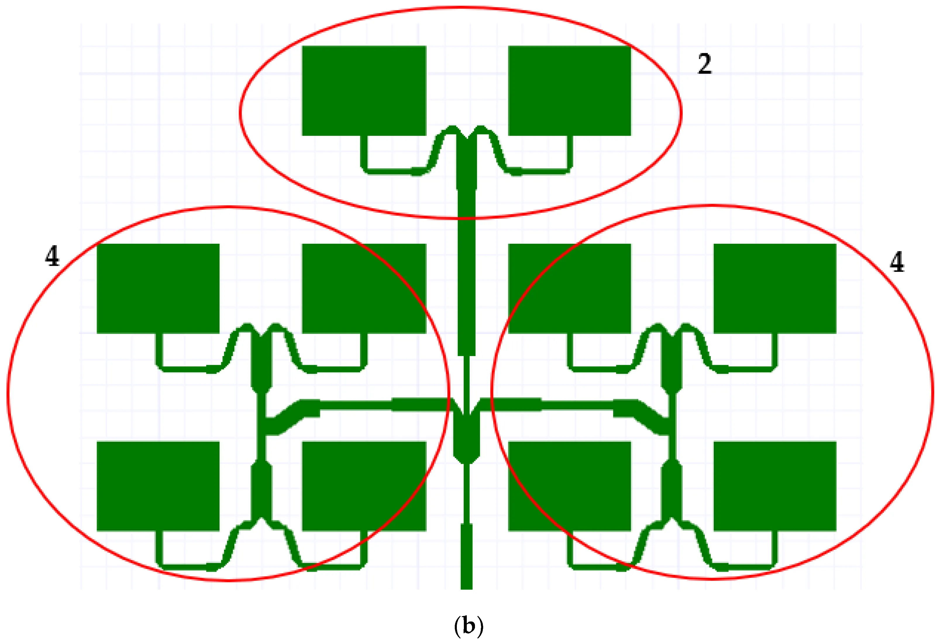
Microstrip antenna design marine systems leverages patch elements etched on low-loss substrates for compact integration with navigation electronics. The patch dimensions resonate at desired frequencies, with substrate height tuning bandwidth and efficiency. Feed lines, often quarter-wave transformers, match antenna impedance to transceiver outputs, minimizing VSWR. Array configurations enhance gain for long-range detection, requiring phase-aligned feeds. Edge effects and surface waves degrade patterns, addressed by cavity backing or aperture coupling. These designs excel in conformal mounting on vessel structures.
Environmental resilience demands robust adhesion and low moisture absorption in dielectrics. Conformal coatings protect against salt spray, per IPC standards for harsh environments. Finite ground planes truncate fields, necessitating absorber treatments in enclosures. Polarization alignment with incoming signals optimizes reception in multipath scenarios. Fabrication tolerances tighten for high-Q resonators, ensuring center frequency stability. Microstrip antenna design marine thus balances performance with manufacturability.
Best Practices for Minimizing Signal Loss in Harsh Marine Environments
Minimizing signal loss PCB starts with selecting substrates exhibiting low dissipation factors at operating frequencies. Smooth copper foils reduce conductor losses from skin effect, while wide traces lower series resistance. Avoiding sharp bends in routing prevents mode conversion and radiation. Transition zones between microstrip and stripline use tapered sections for gradual impedance grading. Thermal vias under high-power components dissipate heat, averting dielectric degradation. These practices sustain signal-to-noise ratios in prolonged marine deployments.
Vibration control involves anchoring traces with anchor points and using flexible substrates in flex-rigid hybrids. Humidity mitigation employs edge plating and sealed enclosures, aligned with IPC-6012 Class 3 for high-reliability boards. EMI shielding via metal pours and ferrite beads suppresses external interference. Power integrity simulations identify droop under load, guiding plane sizing. Routine testing with vector network analyzers confirms loss budgets. Collective adherence yields PCBs resilient to marine rigors.
Troubleshooting Common Issues in High-Frequency Marine PCBs
Signal degradation often traces to via resonances, diagnosed via frequency sweeps revealing nulls at multiples of quarter-wavelength. Adjusting stub lengths or back-drilling mitigates this. Crosstalk spikes indicate inadequate spacing; increasing separation or adding guard traces resolves it. Insertion loss plateaus from dielectric absorption, prompting material swaps within stackup constraints. Ground bounce manifests as jitter; dense decoupling networks stabilize it. Post-assembly, thermal cycling per J-STD standards uncovers latent defects like delamination.
Fabrication variances shift impedances; TDR mapping pinpoints discrepancies for rework. Antenna detuning from nearby metal requires spacing or parasitic elements. Vibration-induced opens demand strain relief in mounting. Systematic logging of S-parameters guides iterative fixes. Field data from deployed systems refines future designs. Troubleshooting reinforces layout robustness.
Conclusion
Advanced high-frequency PCB layout techniques are indispensable for reliable marine navigation systems, integrating impedance control, signal routing, and antenna design seamlessly. Key principles like transmission line theory and loss mechanisms guide practical implementations, from stackups to grounding. Best practices in minimizing signal loss ensure endurance in corrosive, vibrating seas. Engineers applying these methods achieve superior signal integrity marine PCBs, compliant with IPC-2141A and IPC-6012. Future advancements will refine materials and modeling, but foundational engineering remains paramount. Prioritizing these strategies elevates system performance and safety.
FAQs
Q1: What role does impedance control play in high-frequency PCB layout for marine systems?
A1: Impedance control PCB maintains consistent characteristic impedance along signal paths, preventing reflections that distort high-speed data in navigation radars. Proper stackup and trace geometry achieve target values like 50 ohms, verified by TDR. In marine environments, it counters humidity effects on dielectrics. Following IPC-2141A ensures fabrication tolerance. This preserves waveform integrity essential for accurate positioning.
Q2: How can engineers optimize microstrip antenna design marine applications?
A2: Microstrip antenna design marine involves resonant patch sizing on low-loss substrates for GPS or radar bands. Feed matching via microstrip lines minimizes return loss. Array phasing boosts directivity against sea clutter. Conformal coatings protect against salt. Simulations predict patterns, guiding iterations for bandwidth.
Q3: What techniques minimize signal loss PCB in harsh marine conditions?
A3: Minimizing signal loss PCB uses low-Dk materials, smooth conductors, and optimized routing to cut dielectric and skin losses. Ground planes shorten return paths, vias manage transitions. Thermal management prevents degradation. IPC-6012 Class 3 verifies reliability. These sustain SNR over extended operations.
Q4: Why is signal integrity marine PCB critical for navigation reliability?
A4: Signal integrity marine PCB prevents crosstalk and EMI in high-frequency chains, vital for radar echo processing. Layout symmetry and shielding counter vibrations. Testing confirms low BER. Harsh exposure demands robust designs per standards.
References
IPC-2141A — Design Guide for High-Speed Controlled Impedance Printed Boards. IPC.
IPC-6012E — Qualification and Performance Specification for Rigid Printed Boards. IPC, 2017.
J-STD-020E — Moisture/Reflow Sensitivity Classification. JEDEC, 2014.


