Introduction
Spacecraft electronics operate in extreme environments where electromagnetic interference (EMI) and noise can compromise mission success. Radiation from cosmic rays and solar events induces single event upsets in digital circuits, while onboard power converters and RF transmitters generate conducted and radiated noise. Effective PCB layout for noise reduction becomes critical to ensure signal integrity and system reliability. Advanced techniques such as ground plane design, guard rings in space PCBs, trace impedance control, and signal isolation techniques address these challenges systematically. This article explores these methods, providing electrical engineers with structured guidance rooted in engineering principles.
Why Noise and Interference Matter in Spacecraft Electronics
Noise in spacecraft PCBs arises from multiple sources, including crosstalk between adjacent traces, ground bounce from simultaneous switching, and external EMI from antennas or plasma interactions. In vacuum and thermal cycling conditions, poor layout amplifies these effects, leading to bit errors or false triggers in control systems. Reliability demands exceed terrestrial applications, as repair is impossible post-launch. PCB layout for noise reduction directly impacts compliance with high-reliability specifications. Minimizing interference preserves data accuracy in sensors and telemetry links essential for navigation and communication.
Fundamental Mechanisms of Noise in Spacecraft PCBs
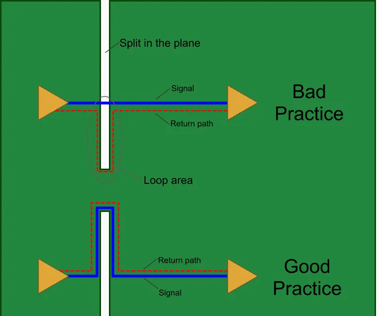
Crosstalk occurs when capacitive or inductive coupling between traces induces unwanted voltages, particularly at high frequencies common in spacecraft data buses. Radiated EMI couples into loops formed by signal returns, while conducted noise propagates through power and ground paths. In space, total ionizing dose effects degrade dielectrics, increasing susceptibility over time. Understanding these mechanisms guides layout choices like minimizing trace lengths and loop areas. Ground bounce, caused by inductance in return paths, further degrades performance during high-current transients.
Ground Plane Design for Optimal Noise Suppression
A continuous ground plane provides a low-impedance return path, reducing inductive loops and shielding sensitive signals from EMI. In multi-layer boards, dedicate inner layers to solid ground planes, ensuring coverage under all signal traces for image plane coupling. Stitch ground planes with vias spaced at less than one-tenth wavelength of the highest frequency to prevent slot antennas. Avoid splitting planes under high-speed signals unless isolated partitions are used with care. IPC-2221C outlines requirements for plane integrity in high-reliability designs. Proper ground plane design forms the foundation of PCB layout for noise reduction.
Related Reading: The Ultimate Guide to Spacecraft Electronics PCB Design Software
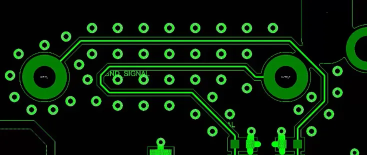
Implementing Guard Rings in Space PCBs
Guard rings encircle sensitive analog circuits, shunting noise currents away from critical nodes via low-impedance paths to ground. Place wide copper rings around amplifiers or ADCs, connected frequently to ground with vias to minimize impedance. In aerospace PCBs, guard rings prevent radiation-induced glitches from coupling into precision measurements. Combine with moats, etched clearances in ground planes, to break stray current paths while maintaining structural integrity. Fabricate rings on multiple layers for enhanced effectiveness. These structures excel in isolating low-level signals from digital noise.
Trace Impedance Control for Signal Integrity
Controlled impedance traces maintain consistent characteristic impedance, preventing reflections that cause ringing and EMI. Use microstrip for outer layers or stripline for inner layers, adjusting width, thickness, and dielectric height accordingly. In spacecraft applications, match 50-ohm single-ended or 100-ohm differential pairs for RF and high-speed digital lines. IPC-2141A provides guidance on calculating and verifying impedance in high-speed designs. Simulate stack-ups early to account for material variations under thermal stress. Trace impedance control ensures clean edges and reduced emissions.
Advanced Signal Isolation Techniques
Partition the PCB into analog, digital, and power zones with separate ground returns to prevent noise cross-contamination. Route sensitive signals orthogonally to potential aggressors and bury them between ground planes for shielding. Employ differential signaling to reject common-mode noise, ideal for long interconnects in avionics. Use ferrite beads or filters at boundaries, but prioritize layout separation. In space, avoid vias in critical paths to minimize parasitics. Signal isolation techniques complement other methods for comprehensive EMI control.
Integrating Techniques into Best Practices
Combine ground planes with impedance-controlled traces by aligning signals parallel to plane edges. Place decoupling capacitors close to IC power pins, with short, wide traces to ground. Minimize via count under clocks and use blind or buried vias where possible. Review layout for symmetry in differential pairs to balance coupling. Perform pre-layout simulations for crosstalk budgets. These practices align with IPC-6012 performance specifications for rigid boards in harsh environments.
Additional Considerations for Spacecraft Reliability
Thermal management influences noise, as CTE mismatches induce stresses that alter impedances. Use symmetric stack-ups to prevent warpage under cycling. Radiation-hardened components require layout tweaks like increased spacing for outgassing. Vibration testing validates mechanical integrity of isolation features. Iterate designs with EMI scans during prototyping.
Conclusion
Mastering PCB layout for noise reduction in spacecraft electronics demands integrated application of ground plane design, guard rings in space PCBs, trace impedance control, and signal isolation techniques. These methods systematically mitigate EMI risks in unforgiving conditions. Electrical engineers benefit from adhering to established principles and standards for robust performance. Implementing them early in the design cycle ensures mission-critical reliability. Future advancements will build on these foundations for even higher frequencies and densities.
FAQs
Q1: What role does ground plane design play in PCB layout for noise reduction?
A1: Ground plane design provides low-impedance returns and shields signals, minimizing loop inductance and EMI coupling. Stitch planes with dense vias to block resonances. In spacecraft, full coverage under traces prevents radiation pickup. Follow guidelines for splits only at zone boundaries. This technique reduces crosstalk by over an order of magnitude in multi-layer boards.
Q2: How do guard rings in space PCBs enhance signal isolation techniques?
A2: Guard rings divert noise currents from sensitive areas via grounded copper paths. Connect them multiply to planes for effectiveness. They complement moats by handling capacitive coupling. In space environments, they guard against glitch propagation. Proper sizing ensures minimal impact on board area.
Q3: Why is trace impedance control essential for spacecraft electronics?
A3: Trace impedance control prevents reflections that distort signals and radiate EMI. Maintain 50 or 100 ohms via stack-up optimization. Space thermal swings demand margin in calculations. It preserves eye diagrams for high-speed links. Verification through TDR confirms compliance.
Q4: What are key best practices for overall noise minimization in space PCBs?
A4: Partition zones, control impedances, and use solid grounds as core practices. Orthogonal routing and short returns limit coupling. Decouple aggressively near sources. Simulate and test iteratively. These ensure interference-free operation per reliability specs.
References
IPC-2221C — Generic Standard on Printed Board Design. IPC, 2023
IPC-2141A — Design Guide for High-Speed Controlled Impedance Circuit Boards. IPC, 2004
IPC-6012DS — Space and Military Avionics Applications Addendum to IPC-6012D Qualification and Performance Specification for Rigid Printed Boards. IPC, 2015
J-STD-001J — Requirements for Soldered Electrical and Electronic Assemblies. IPC, 2024


