Introduction
Telecommunication base stations operate in demanding environments where high-speed data transmission, radiofrequency signals, and substantial power delivery converge. PCB stackup design forms the foundation for these systems, determining signal integrity, thermal performance, and mechanical reliability. In base stations, multilayer PCB designs must accommodate diverse requirements, from gigahertz RF paths to low-voltage digital interfaces and high-current power planes. Poor stackup choices lead to issues like crosstalk, insertion loss, and board warpage, compromising uptime in 24/7 operations. Engineers prioritize PCB stackup design to balance layer count, material properties, and impedance control, ensuring compliance with rigorous performance standards. This article explores advanced strategies for base station PCB layers, focusing on signal integrity stackup and impedance control stackup techniques.

Understanding PCB Stackup Design and Its Critical Role in Base Stations
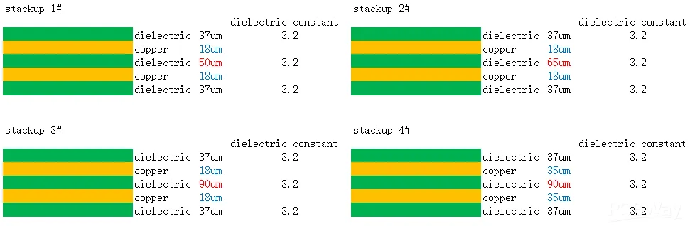
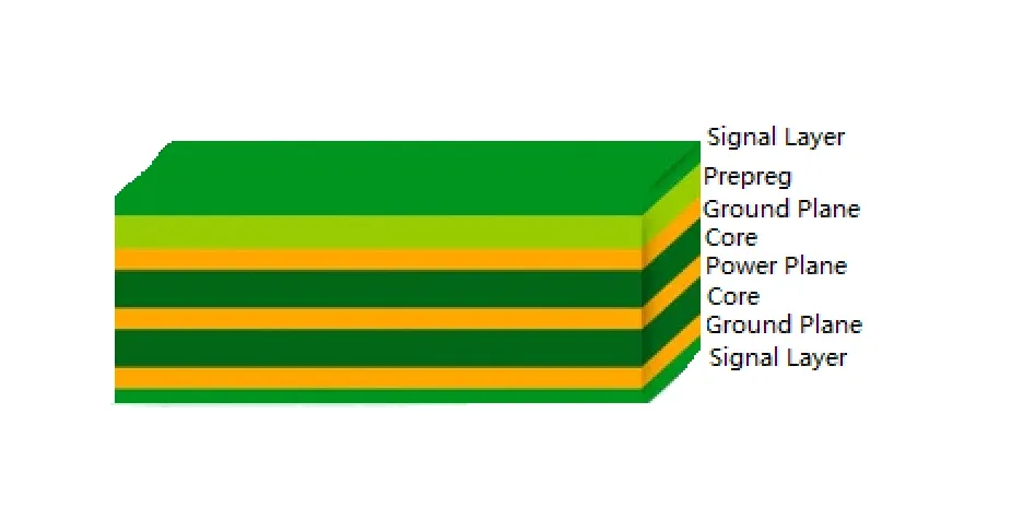
PCB stackup design refers to the strategic arrangement of conductive layers, dielectrics, and planes within a multilayer board. Each layer serves a specific function, such as signal routing, ground reference, or power distribution, influencing overall electrical and mechanical behavior. In telecommunication base stations, base station PCB layers typically range from 12 to 32 or more, supporting complex architectures with RF front-ends, baseband processors, and power amplifiers. These designs demand precise control over dielectric thickness and material constants to maintain characteristic impedance across high-frequency signals. Why does this matter? Base stations handle massive data throughput at frequencies exceeding 10 GHz, where even minor stackup asymmetries cause signal degradation or electromagnetic interference. Optimized multilayer PCB design mitigates these risks, extending equipment lifespan and reducing field failures.
The relevance intensifies with evolving network demands, requiring stackups that integrate mixed-signal environments seamlessly. Signal paths for digital backhaul coexist with analog RF chains, necessitating isolated layers to prevent noise coupling. Mechanical stability becomes paramount as boards endure vibration, thermal cycling, and humidity in outdoor enclosures. Engineers evaluate stackup through simulations and prototypes, correlating layer sequencing to metrics like return loss and eye diagram quality. Ultimately, effective PCB stackup design translates to higher modulation efficiency and lower bit error rates in base station operations.
Core Technical Principles of Advanced Stackup Design
At the heart of advanced PCB stackup design lies the interplay of electrical, thermal, and mechanical principles. Characteristic impedance, governed by the formula Z0 = (87 / sqrt(εr + 1.41)) * log(5.98H / (0.8W + T)) for microstrips, depends on trace width, height, and dielectric constant εr. In impedance control stackup configurations, engineers pair signal layers tightly with reference planes to achieve 50-ohm single-ended or 100-ohm differential impedances consistently. For base station PCB layers, this precision prevents reflections that distort modulated signals in LTE or 5G waveforms. Dielectric materials with low dissipation factor (Df) minimize signal attenuation, crucial for paths exceeding 20 inches at multi-GHz speeds.
Signal integrity stackup principles address crosstalk and mode conversion through stripline or microstrip topologies. Adjacent signal layers introduce broadside coupling, quantified by capacitive and inductive coefficients, so minimum spacing rules apply based on rise times and densities. Ground and power planes act as shields, but their placement affects loop inductance in power delivery networks. In multilayer PCB design, core and prepreg selections influence propagation delay uniformity, ensuring skew below 50 ps across pairs. Thermal conductivity of stackups manages heat from power amplifiers, with vias distributing dissipation to chassis grounds. These mechanisms, when aligned, yield robust performance under varying loads.
Resonance and radiation further complicate high-layer-count stackups. Cavity modes between planes can amplify noise if spacing resonates at operating harmonics, mitigated by stitching vias at lambda/20 intervals. Via transitions introduce discontinuities, modeled as T-networks with parasitics impacting insertion loss by 1-2 dB per transition at 20 GHz. Engineers optimize stub lengths and back-drilling to preserve signal integrity stackup efficacy. Material CTE mismatch between copper and dielectrics induces stress, potentially cracking vias during reflow or operation. Adhering to IPC guidelines ensures stackups withstand these stresses without delamination.
Best Practices for Implementing Optimized Stackups in Base Stations
Practical multilayer PCB design begins with symmetric stackups to counteract warpage from CTE differentials. Pairing outer signal layers with thin dielectrics over thick cores centers the neutral axis, reducing bow and twist to under 0.75% as per industry benchmarks. For base station PCB layers, a common 20-layer configuration might sequence as signal-ground-signal-power, repeating with inner power-ground pairs for decoupling. This arrangement supports dense routing while providing return paths within 5 mils. Impedance control stackup verification uses time-domain reflectometry during fabrication, targeting tolerances of ±10%. Fabricators adjust press cycles to achieve uniform dielectric heights, critical for high-yield production.
Material selection drives signal integrity stackup performance. Low-loss dielectrics with Dk around 3.5 and Df below 0.005 suit RF sections, while higher Dk materials consolidate digital layers. Hybrid stackups blend these, transitioning via controlled-depth routing. Power integrity demands split planes with dense stitching, minimizing impedance below 1 nH per square. Thermal vias under hot components, arrayed at 20-mil pitch, enhance spreading without shorts. Engineers document stackup in fab drawings, specifying sequence, thicknesses, and etch factors for repeatability.
Blind and buried vias optimize density in base station PCB layers, reducing aspect ratios below 10:1 for plating uniformity per IPC-6012 standards. Sequential lamination builds complex structures, enabling embedded capacitors for decoupling. Signal integrity stackup simulations predict PDN noise, guiding capacitor placement at board edges and ICs. Mechanical reliability improves with capped vias and filled structures, resisting fatigue from thermal ramps exceeding 100°C/min. Post-lamination inspections, including cross-sectioning, validate layer alignment within 2 mils. These practices ensure field-deployable boards meeting stringent uptime requirements.
In high-power sections, stackups incorporate heavy copper planes, up to 4 oz/ft2, fused during lamination for current handling over 20A per trace. Cooling channels or thermal pads interface with heatsinks, maintaining junction temperatures below 125°C. EMI suppression layers with frequency-selective planes filter harmonics. Prototype iterations refine designs, correlating measurements to models for production scaling.
Common Challenges and Troubleshooting Strategies
Base stations expose stackups to extremes, revealing challenges like via barrel cracking from z-axis expansion. Troubleshooting involves X-ray and dye-and-peel analysis to pinpoint failures, often tracing to asymmetric builds. Warpage exceeds limits when core-prepreg ratios imbalance, addressed by controlled impedance stackup symmetry and edge clamping during reflow. Signal attenuation spikes at resonances, resolved by chamfered plane splits and moat stitching. J-STD-001 guidelines dictate workmanship for high-reliability assemblies.
Mixed-signal coupling demands guard traces and partitioned grounds, verified through near-field scans. Power droop during transients requires distributed capacitance, modeled in PDN analyzers. Field returns from humidity-induced failures highlight conformal coating needs over exposed layers. Iterative DFM reviews integrate these fixes early.
Conclusion
Advanced PCB stackup design elevates telecommunication base stations from functional to exemplary, harmonizing impedance control stackup, signal integrity stackup, and multilayer PCB design imperatives. Symmetric layering, precise material choices, and rigorous verification practices deliver unmatched performance and reliability. Engineers armed with these principles navigate complexity, ensuring networks thrive under peak loads. Prioritizing these elements minimizes risks, fostering innovation in next-generation deployments.
FAQs
Q1: What is PCB stackup design, and why is it essential for base station PCB layers?
A1: PCB stackup design involves arranging conductive, dielectric, and plane layers to meet electrical and mechanical needs. For base station PCB layers, it ensures high-speed signals propagate with minimal distortion across 12-32 layers. Proper sequencing controls impedance and reduces crosstalk, vital for RF and digital coexistence. This foundation supports reliable operation in harsh environments, preventing failures that disrupt service.
Q2: How does impedance control stackup improve signal integrity in telecom applications?
A2: Impedance control stackup maintains consistent 50/100-ohm lines by specifying dielectric heights and trace geometries. It minimizes reflections and losses at gigahertz frequencies common in base stations. Tight layer pairing with planes provides low-inductance returns, enhancing eye opening. Verification through TDR confirms tolerances, optimizing signal integrity stackup for modulation schemes like OFDM.
Q3: What are key considerations in multilayer PCB design for base stations?
A3: Multilayer PCB design for base stations balances layer count, symmetry, and materials for thermal and SI performance. Symmetric builds prevent warpage, while low-Df dielectrics suit RF paths. Plane placement and via strategies manage power delivery and EMI. Adherence to IPC standards ensures manufacturability and reliability in high-volume production.
Q4: How can engineers optimize base station PCB layers for thermal reliability?
A4: Optimize base station PCB layers with thermal vias, heavy copper planes, and high-conductivity cores to dissipate amplifier heat. Symmetric stackups aid uniform expansion, reducing stress. Simulations predict hotspots, guiding heatsink interfaces. This approach maintains performance during prolonged high-power operation without degradation.
References
IPC-2221B — Generic Standard on Printed Board Design. IPC, 2009
IPC-6012E — Qualification and Performance Specification for Rigid Printed Boards. IPC, 2017
J-STD-001H — Requirements for Soldered Electrical and Electronic Assemblies. IPC, 2020


