Introduction
Power supply printed circuit boards form the backbone of electronic systems, delivering stable voltage and current to downstream circuits. Optimizing their layout directly impacts overall system efficiency, thermal management, and electromagnetic compatibility. Engineers face challenges like high current densities, switching noise, and heat dissipation that demand precise design strategies. This article explores advanced techniques grounded in engineering principles to enhance power supply PCB performance. By focusing on component placement, routing, and noise mitigation, designers can achieve reliable operation under demanding conditions. Key areas include power supply PCB layout best practices, power supply PCB grounding techniques, and methods for reducing EMI in power supply PCBs.
Why Power Supply PCB Layout Matters
Effective power supply PCB layout ensures minimal voltage droop, reduced parasitic inductance, and controlled electromagnetic emissions. In high-power applications, improper trace sizing or plane splits can lead to hotspots and efficiency losses exceeding acceptable thresholds. Layout decisions influence power integrity, where ripple and transient response determine system stability. Grounding schemes prevent noise coupling between power and signal domains, preserving signal fidelity. Adhering to established guidelines minimizes rework during prototyping and certification phases. Ultimately, optimized layouts extend product lifespan and reduce field failures in industrial and consumer electronics.
Fundamental Principles of Power Delivery in PCBs
Power delivery begins with understanding current paths and their interaction with board materials. High-frequency switching in DC-DC converters generates magnetic fields that induce voltage spikes if loop areas are large. Conductors must carry current without excessive temperature rise, guided by standards like IPC-2152 for determining trace widths based on copper thickness and ambient conditions. Plane structures provide low-impedance returns, essential for transient currents. Layer stackup choices affect capacitance between power and ground, stabilizing voltage rails. These principles form the basis for layout decisions that balance electrical, thermal, and mechanical constraints.
Component Placement Strategies
Strategic placement groups high-current components like inductors, capacitors, and switches to minimize trace lengths. Input capacitors should sit closest to the switching device to supply ripple current effectively. Output sections require separation from input to avoid noise propagation through shared paths. Sensitive feedback loops demand isolation from noisy power nodes. Thermal vias under hot components channel heat to inner layers or heatsinks. This arrangement reduces parasitic effects and supports power supply PCB layout best practices by promoting short, wide paths for DC currents.
Power Supply PCB Grounding Techniques
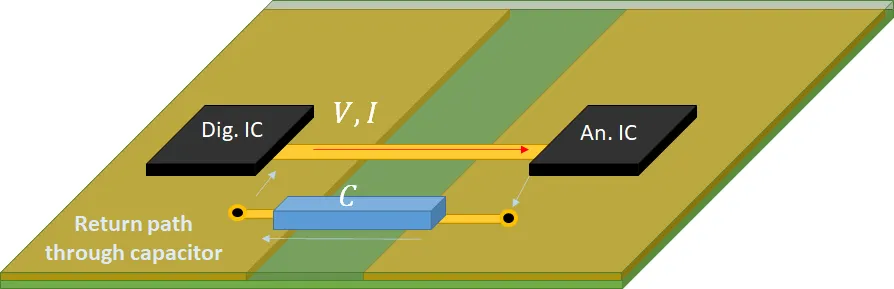
Power supply PCB grounding techniques rely on low-impedance paths to return currents without creating potential differences. A solid ground plane on an inner layer serves as the primary reference, minimizing inductance compared to routed grounds. For mixed-signal supplies, split planes connect at a single point near the power entry to block digital noise from analog sections. Stitching vias around splits maintain plane integrity for high-frequency returns. Kelvin connections for sense lines preserve accuracy by avoiding voltage drops along shared grounds. These methods align with design standards to ensure stable operation and reduce common-mode noise.
Star grounding suits low-frequency supplies where multiple returns converge at one chassis point, preventing loops. Multi-point grounding excels in high-speed designs by using planes for distributed low-inductance paths. Hybrid approaches combine both, with dedicated analog grounds tied to the main plane strategically. Engineers must simulate ground bounce to validate choices under load steps. Proper implementation cuts noise floors by orders of magnitude, enhancing overall EMC performance.
Reducing EMI in Power Supply PCBs
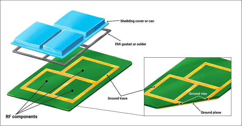
Reducing EMI in power supply PCBs starts with minimizing current loop areas, as radiated emissions scale with loop size and di/dt. Switching loops between high-side drivers, MOSFETs, and return paths should enclose the smallest possible area. Adjacent power and ground planes form a stripline structure that shields fields from external layers. Guard rings around noisy components divert stray fields, while ferrite beads on cables suppress conducted emissions. Filter placement at board edges blocks ingress and egress of differential-mode noise. These techniques comply with general EMC principles and prevent redesign iterations.
Trace routing avoids parallel runs between hot signals and victims, using orthogonal directions where crossings occur. Wide power traces reduce series resistance, damping resonances that amplify emissions. Vias for high-current transitions require multiple parallels to spread current evenly. Snubbers across switches absorb switching transients before they radiate. Pre-layout EMI simulations predict field strengths, allowing iterative refinements. Consistent application yields boards passing regulatory tests on first pass.
Layer Stackup Optimization
Optimal layer stackups dedicate inner layers to power distribution and ground returns. Power planes adjacent to ground planes maximize distributed capacitance, filtering high-frequency noise. Signal layers sandwich between planes for shielding, with minimal vias piercing sensitive areas. Asymmetric stackups risk warpage, so balanced copper distribution maintains flatness per IPC-6012 specifications. Thicker dielectrics between signal layers control crosstalk in multi-layer boards. Simulations verify impedance profiles matching component requirements.
Trace Routing and Width Selection
Power traces demand generous widths to handle RMS currents without exceeding 20-degree temperature rises. IPC-2152 charts guide sizing, factoring external airflow and board thickness. High-frequency paths use controlled impedance to match source and load, preventing reflections. Avoid 90-degree bends; use 45-degree chamfers to reduce reflections and manufacturing defects. Differential pairs for synchronous rectifiers maintain equal lengths for balance. Post-routing DRCs enforce spacing rules from IPC-2221 to prevent arcing under voltage stress.
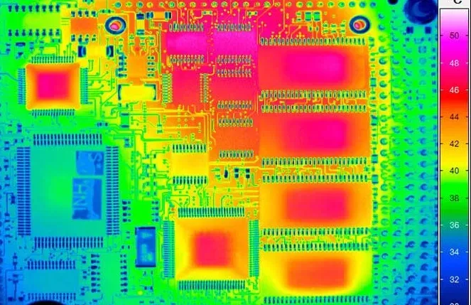
Thermal Management Integration
Thermal vias arrays under ICs and passives conduct heat efficiently to copper pours. Plane cuts around vias prevent shorting in multi-layer designs. Heatsink mounting pads align with component centers for uniform pressure. Convection paths remain unobstructed by routing over pours. Junction-to-ambient modeling predicts hotspots early. Integrated thermal strategies complement electrical optimization for sustained performance.
Advanced Simulation and Verification
Field solver tools model inductance and capacitance in complex geometries. Time-domain simulations capture switching transients and ripple. Post-layout extractions feed into system-level analysis for PDN integrity. Prototype measurements with scopes and spectrum analyzers validate predictions. Iterative tweaks refine the design before volume production. This workflow embodies power supply PCB layout best practices for modern high-density boards.
Conclusion
Mastering power supply PCB layout requires integrating placement, grounding, routing, and EMI controls into a cohesive design. Power supply PCB grounding techniques and strategies for reducing EMI in power supply PCBs directly address common failure modes. Adhering to standards like IPC-2221 and IPC-2152 ensures manufacturability and reliability. Engineers benefit from simulations and prototypes to fine-tune implementations. These advanced techniques enable compact, efficient power supplies that meet stringent performance demands. Prioritizing layout optimization yields systems with superior noise immunity and longevity.
FAQs
Q1: What are the key power supply PCB layout best practices for high-current designs?
A1: Power supply PCB layout best practices emphasize wide traces sized per IPC-2152, short switching loops, and dedicated planes. Place input filters near converters and separate noisy sections. Use thermal vias for heat spreading. Verify with PDN analysis to ensure low impedance across frequencies. These steps minimize droop and hotspots effectively.
Q2: How do power supply PCB grounding techniques reduce noise coupling?
A2: Power supply PCB grounding techniques employ solid planes for low-inductance returns and single-point ties for splits. Stitching vias bridge high-frequency currents around divisions. Analog grounds isolate from digital noise sources. Kelvin sensing avoids IR drops in feedback paths. This setup lowers common-mode interference significantly.
Q3: What methods are effective for reducing EMI in power supply PCBs?
A3: Reducing EMI in power supply PCBs involves minimizing loop areas, using adjacent planes for shielding, and adding edge filters. Orthogonal routing prevents coupling, while snubbers dampen transients. Guard traces and ferrites further attenuate emissions. Simulations guide optimizations before fabrication. Compliance follows naturally from these practices.
Q4: Why is layer stackup critical in power supply PCB design?
A4: Layer stackup in power supply PCBs provides interplane capacitance for decoupling and shields signals from emissions. Balanced copper prevents warpage per IPC-6012. Power-ground adjacency controls PDN impedance. Signal routing between planes reduces crosstalk. Proper sequencing supports high-density integration reliably.
References
IPC-2221B — Generic Standard on Printed Board Design. IPC.
IPC-2152B — Standard for Determining Current Carrying Capacity in Printed Board Design. IPC.
IPC-6012DS — Qualification and Performance Specification for Rigid Printed Boards. IPC.
J-STD-001H — Requirements for Soldered Electrical and Electronic Assemblies. IPC, J-STD.


