Introduction
Navigation system printed circuit boards handle sensitive radio frequency signals that demand high precision and reliability. Electromagnetic interference, or EMI, poses a significant challenge in these designs, as it can disrupt signal integrity and lead to positioning errors. In applications like global positioning systems and inertial navigation, even minor interference can compromise performance. Engineers must employ advanced techniques to mitigate EMI while maintaining compact layouts and cost efficiency. This article explores key strategies tailored for navigation PCBs, focusing on proven methods to enhance electromagnetic compatibility.
Why EMI Matters in Navigation System PCBs
Navigation PCBs process signals in the gigahertz range, making them particularly susceptible to radiated and conducted emissions. External sources such as nearby power lines or internal noise from digital clocks can couple into RF paths, causing phase shifts or amplitude variations. These effects degrade receiver sensitivity and increase time-to-first-fix durations. Compliance with electromagnetic compatibility requirements ensures systems operate reliably in diverse environments, from automotive to aerospace. Reducing EMI not only improves accuracy but also prevents false locks on satellite signals. For electric engineers, understanding these implications guides robust design choices from the outset.
Sources of EMI in Navigation System PCBs
EMI in navigation PCBs arises primarily from high-speed digital circuits generating harmonics that overlap with RF bands. Switching power supplies produce conducted noise that propagates through power planes. Trace loops act as antennas, radiating energy based on their area and frequency. Improper grounding allows common-mode currents to flow, exacerbating interference. In dense layouts, crosstalk between adjacent traces further amplifies issues. Identifying these sources early through simulation and layout review forms the foundation for effective mitigation.
Navigation PCB Grounding Techniques
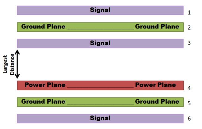
Effective navigation PCB grounding techniques start with dedicated ground planes that provide low-impedance return paths for all signals. Splitting planes between analog RF sections and digital logic minimizes noise coupling, while stitching vias connect them at strategic points to avoid slots. Guard rings around sensitive components shunt stray fields to ground. Multi-layer boards benefit from adjacent power and ground planes forming stripline structures that contain fields. As outlined in IPC-2221 guidelines, consistent ground referencing reduces loop inductance. Engineers should verify plane integrity during stackup definition to ensure uniform current distribution.
Placing decoupling capacitors close to IC pins further enhances grounding by bypassing high-frequency noise directly to the plane. Via fences along board edges or trace perimeters create shielded barriers. In navigation designs, separating GNSS receiver grounds from processor grounds prevents digital hash from desensitizing the front-end. Thermal vias under power devices aid heat dissipation without compromising ground continuity. These techniques collectively lower emissions by tens of decibels in critical frequency bands.
Navigation PCB EMI Shielding
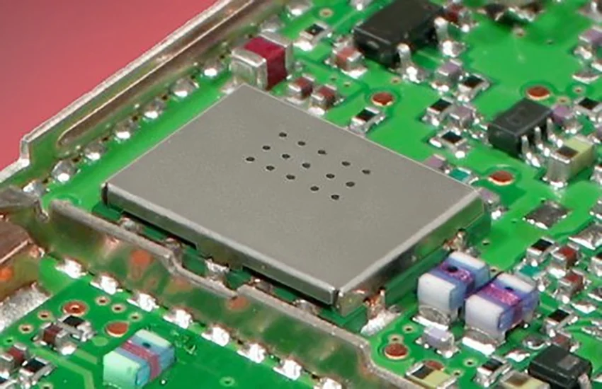
Navigation PCB EMI shielding involves enclosures and on-board methods to contain electromagnetic fields. Metal cans over RF modules block external ingress while grounded lids seal the structure. Ground via arrays, spaced at less than one-tenth wavelength, surround sensitive traces to form Faraday cages. Embedded shielding films in multi-layer boards offer compact alternatives for high-density designs. Careful lid attachment with conductive gaskets ensures low-resistance paths. Shielding effectiveness depends on seam integrity and material conductivity.
For flexible integration, selective shielding targets hotspots like crystal oscillators. Vias connected to ground planes under shields prevent resonance. In navigation systems, shielding GNSS antennas from onboard transmitters maintains link margins. Combining shielding with layout segregation yields synergistic reductions. Engineers must balance shielding with thermal management to avoid hotspots.
Navigation PCB Filter Design
Navigation PCB filter design employs passive networks to attenuate noise at entry points. Pi-filters using capacitors and inductors on power lines block conducted EMI effectively. Ferrite beads in series with signals present high impedance to common-mode currents above cutoff frequencies. Placement within millimeters of noise sources maximizes suppression before propagation. Component values derive from impedance matching and frequency response curves. Multi-stage filters handle broadband threats in navigation environments.
Low-pass configurations suit DC power rails feeding receivers. Bypass capacitors in parallel shunts high frequencies to ground. Simulation tools validate filter performance against expected harmonics. In practice, surface-mount ferrites reduce parasitics compared to wire-wound types. Regular attenuation measurements confirm design margins. These filters integrate seamlessly with other techniques for comprehensive protection.
Navigation PCB Differential Signaling
Navigation PCB differential signaling transmits data as complementary pairs, inherently rejecting common-mode noise. Receivers compare signals to nullify ground bounce and external interference. Matched trace lengths and impedances preserve balance, minimizing skew. Tightly coupled pairs reduce radiated emissions by confining fields between conductors. This approach suits high-speed interfaces like LVDS for data transport in navigation modules. Conversion to single-ended occurs only at endpoints with care.
Routing differential pairs on inner layers shields them from surface noise. Length tuning compensates for vias. Pre-emphasis drivers counteract losses in long runs. In GNSS applications, differential signaling enhances serial peripheral interfaces. Pair twisting in cables extends benefits off-board. Overall, it simplifies shielding needs while boosting noise immunity.
Navigation PCB Common Mode Choke
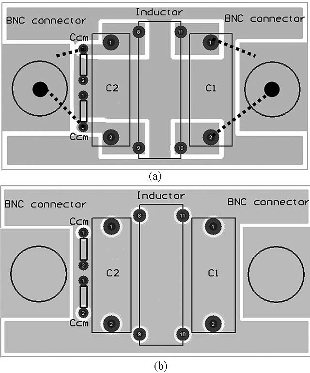
A navigation PCB common mode choke uses coupled windings to impede common-mode currents while passing differential signals. Placed on cable interfaces or inter-board links, it suppresses noise from external sources. Core materials like manganese-zinc ferrites target specific bands. Bifilar windings ensure tight coupling for balance. Saturation current ratings prevent distortion under load. Selection considers impedance curves matching threat spectra.
Integration near connectors minimizes stub effects. Multiple chokes in series handle multi-path noise. In navigation systems, they protect Ethernet or USB from injecting EMI into RF sections. Testing with LISN verifies insertion loss. Combined with filters, chokes form robust input stages. Proper PCB landing pads avoid resonance.
Integrating Best Practices for Optimal EMI Performance
Successful EMI reduction in navigation PCBs requires holistic layout strategies. Partitioning the board into zones isolates noisy digital from quiet analog areas. Shortening high-speed traces and avoiding right angles curbs radiation. Power plane cutouts under ICs prevent resonance. Cross-talk mitigation via spacing rules exceeds minimums. Stackup optimization with microstrip for low-speed and stripline for high-speed controls impedance.
Component orientation aligns decoupling caps for shortest paths. Board edges feature ground stitching to contain edge diffraction. Simulation iterates designs pre-prototype. As per IEC 61000 standards for electromagnetic compatibility, these practices ensure field limits compliance. Field probing post-assembly pinpoints residuals. Iterative refinement achieves certification margins.
Troubleshooting EMI Issues in Navigation PCBs
Common EMI symptoms include intermittent signal loss or elevated phase noise. Spectrum analysis identifies culprit frequencies matching clocks. Near-field probes localize sources. Adjusting ground stitching resolves slot antennas. Filter redesign tackles conducted spikes. Shield seam audits fix leaks.
Differential pair imbalance shows as eye closure. Choke replacement restores balance. Multi-point grounding equalizes potentials. Documentation of fixes aids future designs. Systematic diagnosis prevents recurrence.
Conclusion
Advanced techniques like navigation PCB grounding techniques, EMI shielding, filter design, differential signaling, and common mode chokes form a layered defense against interference. Logical implementation from stackup to assembly yields reliable performance. Engineers benefit from structured approaches aligned with industry standards. Prioritizing these methods minimizes redesign cycles and enhances system integrity. Navigation systems thus achieve precision in demanding environments.
FAQs
Q1: What are the most effective navigation PCB grounding techniques for EMI reduction?
A1: Navigation PCB grounding techniques include solid planes, stitching vias, and partitioned zones for analog and digital sections. These provide low-impedance returns and contain fields. Guard traces and decoupling capacitors further suppress noise. Following IPC-2221 guidelines ensures consistency. Implementation reduces emissions significantly in high-frequency designs.
Q2: How does navigation PCB differential signaling help with EMI?
A2: Navigation PCB differential signaling rejects common-mode noise by comparing paired signals. Matched impedances and tight coupling confine fields, lowering radiation. It suits high-speed data links in GNSS modules. Routing on inner layers enhances shielding. This technique simplifies overall EMI management.
Q3: When should you use a navigation PCB common mode choke?
A3: Use a navigation PCB common mode choke on interfaces like cables or buses prone to external noise. It blocks common currents while passing differential signals. Select based on frequency and current ratings. Placement near connectors maximizes effectiveness. Pairing with filters bolsters protection.
Q4: What role does navigation PCB filter design play in EMI shielding?
A4: Navigation PCB filter design attenuates conducted noise via pi-networks and ferrites near sources. Low-pass types suit power rails, bypassing highs to ground. Broadband response handles harmonics. Proximity minimizes parasitics. Integration with shielding completes the strategy.
References
IPC-2221 — Generic Standard on Printed Board Design. IPC, 2012
IEC 61000-6-1 — Electromagnetic compatibility (EMC) - Part 6-1: Generic standards - Immunity for residential, commercial and light-industrial environments. IEC, 2016
IPC-6012DS — Qualification and Performance Specification for Double-Sided Flexible Printed Boards. IPC, 2015


