Introduction
Rigid-flex printed circuit boards combine the durability of rigid sections with the flexibility of polyimide-based flex areas, enabling compact designs in applications like wearables, medical devices, and aerospace systems. The flex-to-rigid transition zone represents a critical interface where mechanical stresses concentrate during bending, potentially leading to failures such as trace cracking or delamination. Proper bend radius management in this zone ensures long-term reliability by distributing stresses evenly across the flex material. Engineers must prioritize rigid-flex PCB bend radius calculation to avoid exceeding material limits, as insufficient radius amplifies flex PCB bending stress and compromises signal integrity. This article explores the principles behind these calculations, drawing on established design standards, and provides practical strategies for rigid-flex transition zone design. By minimizing stress in flex PCBs, designers can achieve robust performance without over-engineering the stack-up.
What Are Flex-to-Rigid Transition Zones and Why Does Bend Radius Matter?
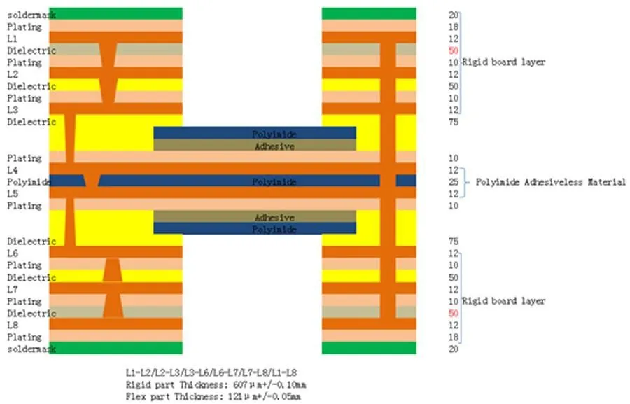
Flex-to-rigid transition zones are the boundary regions where the rigid substrate, typically FR-4, interfaces with the flexible polyimide layers, often incorporating coverlay and adhesive for continuity. These zones experience high strain during assembly or operation because the flex section must curve while the rigid part remains stationary, creating shear and tensile forces at the junction. Bend radius, defined as the smallest radius of curvature the flex can achieve without damage, directly influences the magnitude of these forces; a smaller radius induces higher localized stress. In rigid-flex designs, ignoring bend radius leads to fatigue cracking in copper conductors or substrate tears over repeated cycles. Industry standards like IPC-2223 outline guidelines for these zones to prevent such issues, emphasizing the need for controlled flexing. Ultimately, optimal bend radius selection balances space constraints with mechanical integrity, extending the service life of the assembly.
The relevance intensifies in dynamic applications where the PCB undergoes frequent bending, such as in folding electronics. Poor transition design exacerbates flex PCB bending stress, accelerating failure modes like hillocking in copper foils. Engineers targeting electric applications must integrate bend radius considerations early in the layout phase to comply with performance specs.
Technical Principles of Bending Stress in Flex PCBs
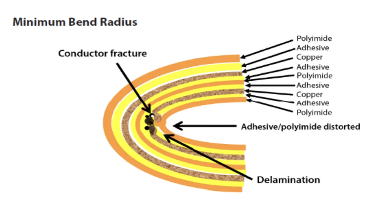
Bending a flex PCB subjects the copper conductors and dielectric to tensile and compressive strains, with maximum stress occurring at the outer and inner fibers of the bend. The strain ε is proportional to the distance from the neutral axis and inversely proportional to the bend radius R, following the basic relation ε = z / R, where z is the distance to the neutral axis. For thin copper layers, this strain translates to bending stress σ = E ε, with E as the modulus of elasticity of the material. Copper's ductility limits the allowable strain to avoid cracking, typically dictating larger radii for thicker stacks or dynamic use. In multilayer flex, the neutral axis shifts due to asymmetric materials, complicating stress distribution and necessitating symmetrical constructions where possible.
Flex PCB bending stress peaks at conductor edges and vias, where stress risers amplify local deformation. Transition zones compound this by introducing material discontinuities, such as abrupt coverlay termination, leading to peel stresses. Finite element analysis often reveals hotspots here, confirming that gradual geometry changes mitigate concentrations. Adhesive shear between layers further influences failure thresholds, as insufficient bonding allows slippage under repeated flexing.
Rigid-Flex PCB Bend Radius Calculation Methods
Rigid-flex PCB bend radius calculation starts with determining the total flex thickness h, including copper, polyimide, and coverlay. Standards like IPC-2223 provide ratio tables where minimum R = N × h, and N varies by layer count and application type: lower for static bends (one-time installation) and higher for dynamic (repeated flexing). For instance, single-layer static designs use ratios around 10:1, while multilayer dynamic may require 100:1 or more to keep strains below copper fatigue limits. Engineers calculate h precisely from stack-up drawings, accounting for plating and adhesives, then select N conservatively based on expected cycles.
To implement, first classify the bend: static for fixed positions post-assembly, semi-dynamic for occasional movement, or full dynamic for continuous flexing. Apply the IPC-2223 ratio, then verify with strain limits; if ε exceeds 0.3% for copper, increase R. Software tools simulate this, but manual checks ensure compliance. Transition zones demand extra margin, often 20% larger R, to accommodate rigid anchoring effects.
- 1 Layer - Static Ratio (N): 6-10; Dynamic Ratio (N): 100+
- 2 Layers - Static Ratio (N): 10-20; Dynamic Ratio (N): 150+
- Multilayer - Static Ratio (N): 20-35; Dynamic Ratio (N): 200+
This list illustrates typical ranges from design guidelines, adjustable per specific materials.
Best Practices for Rigid-Flex Transition Zone Design
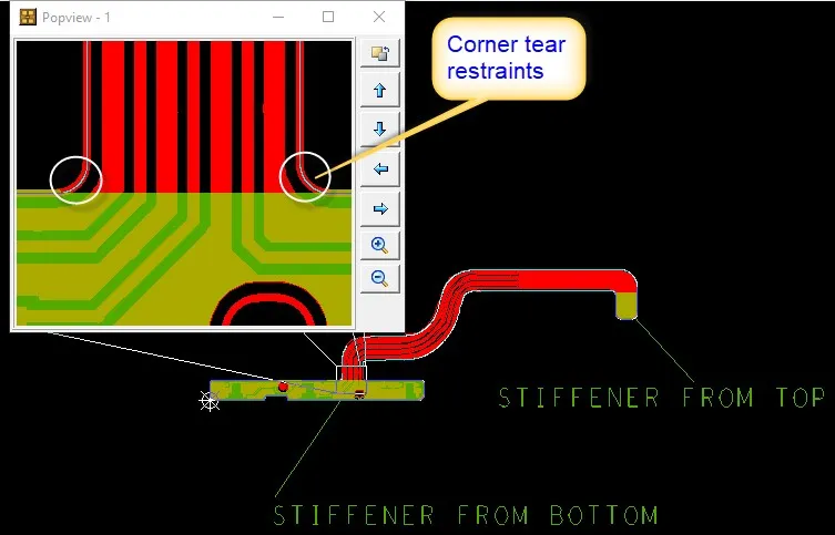
Effective rigid-flex transition zone design begins with smooth contouring: use curved outlines rather than sharp corners to distribute stresses evenly. Extend coverlay 0.5-1 mm into rigid areas for seamless overlap, preventing delamination as per IPC-6013 inspection criteria. Place tear stops, such as slotted patterns in the flex, 3 mm from the rigid edge to control crack propagation if initiated. Avoid vias, pads, or components within 1.5 mm of the transition to eliminate stress risers; route signals straight across the zone with wide traces.
Symmetrical stack-ups in flex sections minimize neutral axis shift, reducing interlaminar shear. Incorporate anchor tabs or fingers that interlock rigid and flex for positive mechanical retention. For high-reliability, add strain-relief features like serpentine traces in the zone, allowing compliant deformation. Prototype testing, including bend cycle evaluations, validates the design before production scaling.
Advanced Techniques for Minimizing Stress in Flex PCBs
Beyond basics, optimize copper thickness: thinner foils (18-35 μm) permit tighter radii by lowering peak strain. Use rolled annealed copper over electrodeposited for better ductility in repeated bends. In transition zones, gradual stiffener tapering over 5-10 mm transitions rigid to flex properties smoothly. Finite element modeling predicts stress hotspots, guiding iterations.
For dynamic apps, segmented flex with multiple bends shares load, halving individual radii needs. Coverlay slits parallel to bend lines relieve compression. Post-fabrication, controlled baking preconditions materials, enhancing flex life. These techniques, aligned with standards, yield 2-5x cycle improvements without added cost.
Conclusion
Mastering bend radius in flex-to-rigid transition zones safeguards rigid-flex PCBs against premature failure by controlling flex PCB bending stress. Through systematic rigid-flex PCB bend radius calculation using IPC guidelines, engineers ensure strains stay within material limits. Implementing rigid-flex transition zone design best practices, like smooth geometries and strategic features, minimizes stress concentrations effectively. Prioritizing these elements delivers reliable, compact assemblies for demanding electric engineering applications. Design with foresight, validate rigorously, and reference standards to optimize performance.
FAQs
Q1: How do you perform rigid-flex PCB bend radius calculation for a static application?
A1: Start by measuring total flex thickness h from the stack-up. Consult IPC-2223 for the appropriate ratio N based on layers, typically 6-35 for static bends. Multiply R = N × h, adding margin for transitions. Verify strain ε = (copper thickness / 2) / R remains below 0.5%. This method ensures safe installation without cracking.
Q2: What causes high flex PCB bending stress in transition zones?
A2: Material discontinuities at the rigid-flex interface create strain gradients during bending. Abrupt edges or vias act as stress risers, amplifying tensile forces in copper. Asymmetric stacks shift the neutral axis, increasing shear. Smooth curves and overlaps per design standards distribute loads evenly, reducing peak stresses significantly.
Q3: What are key rigid-flex transition zone design rules for minimizing stress?
A3: Use curved boundaries, extend coverlay into rigid areas, and add tear stops 3 mm from edges. Avoid features like vias near the zone; opt for wide, straight traces. Symmetrical flex stack-ups prevent warping. These practices comply with IPC-6013 and extend flex life under repeated bending.
Q4: How can engineers minimize stress in flex PCBs during dynamic flexing?
A4: Select higher bend ratios (100:1+) from IPC-2223, thinner copper, and ductile materials. Implement serpentine routing and slit coverlays for compliance. Simulate with FEA to identify hotspots. Gradual transitions and load-sharing segments further reduce fatigue, ensuring reliability in high-cycle environments.
References
IPC-2223E — Sectional Design Standard for Flexible/Rigid-Flexible Printed Boards. IPC, 2020
IPC-6013E — Qualification and Performance Specification for Flexible/Rigid-Flexible Printed Boards. IPC, 2021
IPC-2221G — Generic Standard on Printed Board Design. IPC, 2012


