Introduction
Curvilinear PCBs represent an evolution in printed circuit board design, incorporating organic shapes and curved elements into traditionally rectangular layouts. These boards feature non-linear outlines, flowing trace patterns, and integrated curves that align with modern product enclosures demanding ergonomic or compact forms. Engineers increasingly turn to curvilinear PCB design to achieve seamless integration in devices where flat boards fall short. Unlike standard rigid PCBs, organic PCB shapes allow for aesthetic appeal while maintaining electrical performance. This guide explores the principles, practices, and applications of curvilinear PCBs, positioning them as viable flexible PCB alternatives for static curved configurations. By mastering these techniques, designers can unlock advanced PCB applications in wearables, automotive, and medical sectors.
The push toward curvilinear designs stems from consumer demands for sleeker, more intuitive electronics. Traditional rectangular boards often require adapters or wasteful space in curved housings, leading to inefficiencies. Curvilinear approaches optimize material use and enhance signal integrity through smoother routing. As manufacturing tolerances improve, these boards become feasible for production volumes. This article provides logical, step-by-step insights for electric engineers navigating curvilinear PCB design.
What Are Curvilinear PCBs and Why Do They Matter?
Curvilinear PCBs are rigid or rigid-flex boards defined by curved board outlines, arc-based traces, and irregular contours that mimic natural forms. The term "curvilinear" refers to the use of arcs, splines, and polygons in CAD to create flowing geometries, departing from orthogonal grids. Organic PCB shapes enable boards to conform to cylindrical, spherical, or ergonomic enclosures without dynamic flexing. These designs matter because they address limitations of rectangular PCBs in space-constrained environments, offering curved PCB benefits like maximized usable area and reduced weight.
In industry contexts, curvilinear PCBs gain relevance for applications requiring form-factor innovation. For instance, in IoT sensors or lighting modules, a round or wave-shaped board fits precisely into housings, eliminating gaps and improving thermal flow. They serve as flexible PCB alternatives where repeated bending is unnecessary, avoiding fatigue issues in polyimide substrates. Designers value them for signal performance, as curved traces in RF sections minimize reflections compared to sharp corners. Overall, these boards expand design freedom while adhering to manufacturability constraints.
The relevance extends to sustainability, as organic shapes reduce scrap in panelization when optimized. Engineers must weigh trade-offs in handling and assembly, but the payoff lies in product differentiation. As enclosures evolve toward biomorphic profiles, curvilinear PCB design becomes essential for competitive electronics.
Technical Principles of Curvilinear PCB Design
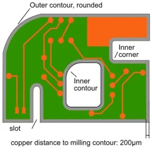
Curvilinear PCB design begins with defining the board outline using CAD tools capable of arcs and Bezier curves. Engineers draw the perimeter as a closed polygon incorporating radii greater than tooling limits, typically starting with 0.5 mm for milling bits. Component placement follows, prioritizing symmetry to balance mechanical stress and thermal expansion. Traces then route organically, employing curved segments for high-frequency lines to preserve impedance. Power and ground planes adapt via polygon pours that hug the irregular edges, ensuring uniform coverage without islands.
For multilayer curvilinear boards, stackup planning accounts for via staggering around curves to avoid drill breakout. Signal integrity benefits from curved bends in RF routing, where a radius of three times the trace width reduces capacitance variations. Simulations validate return loss, showing curved paths outperform 45-degree miters above 10 GHz. Organic PCB shapes demand precise pad arrays aligned to contours, with fiducials offset for optical registration. This structured approach ensures reliability under IPC-2221 guidelines for generic printed board design.
Layer alignment poses unique challenges in curvilinear layouts, as drill misalignment amplifies at edges. Engineers mitigate this by expanding clearances near curves and using blind vias selectively. Curved traces enhance aesthetics in visible applications, like LED arrays, while maintaining 50-ohm impedance through width consistency.
Manufacturing Considerations and Best Practices
Manufacturing curvilinear PCBs requires specialized routing for outlines, using CNC mills with tapered bits to achieve smooth radii. Etching handles internal curved traces via standard photolithography, though finer features benefit from laser direct imaging for sub-100 micron lines. Panelization optimizes yield by nesting organic shapes efficiently, often with V-scoring adapted for arcs. Fixturing during assembly uses custom pallets to secure irregular forms, preventing warpage under reflow.
Best practices include verifying Gerber files for outline accuracy, with step-and-repeat adjusted for curves. IPC-6012 specifications guide qualification, emphasizing edge roughness below 0.1 mm and no delamination at contours. Solder mask registration tolerates slight offsets, but legends avoid sharp bends to prevent cracking. Testing incorporates bend fixtures for static curves, confirming continuity post-milling.
Engineers should collaborate early with fabricators on DFM, specifying minimum radius and tab placements. For multilayer builds, sequential lamination preserves outline integrity. These steps ensure high yields, typically matching rectangular boards when rules are followed.
Curved PCB Benefits and Advanced Applications
Curved PCB benefits include superior space utilization in non-rectangular volumes, ideal for cylindrical housings in sensors or displays. They reduce connector needs by integrating directly into curves, lowering assembly costs and failure points. In RF modules, curved traces minimize radiation, supporting advanced PCB applications up to mmWave frequencies. As flexible PCB alternatives, rigid curvilinear boards offer longevity without cyclic fatigue, suiting static bends in wearables or dashboards.
Applications span automotive lighting panels, where wave-shaped boards distribute LEDs uniformly along curves. Medical devices employ round PCBs for endoscopes, maximizing sensors in tight radii. Consumer electronics like smart speakers use organic shapes for acoustic optimization. Aerospace benefits from lightweight contours reducing inertia in gimbals.
In wearables, rigid-flex hybrids combine curvilinear rigid sections with flex tails, enabling wrist-conforming profiles. These designs enhance user comfort and battery life through efficient packing.
Challenges and Troubleshooting in Curvilinear Design
Key challenges include reduced panel efficiency, dropping yields by 20-30 percent without optimization. Handling thin curved boards risks breakage, necessitating edge rails or carriers. Assembly pick-and-place struggles with fiducial detection on arcs, requiring enhanced lighting.
Solutions involve symmetrical designs per IPC-A-600 acceptability criteria and simulation-driven routing. Custom stencils accommodate contours, while conformal coating protects edges. Troubleshooting focuses on iterative prototyping to refine radii.
Conclusion
Curvilinear PCB design empowers engineers to create organic PCB shapes that deliver curved PCB benefits in advanced applications. By following structured principles, best practices, and standards, designers overcome manufacturing hurdles effectively. These boards stand as practical flexible PCB alternatives, blending form and function seamlessly.
FAQs
Q1: What distinguishes curvilinear PCB design from standard rectangular layouts?
A1: Curvilinear PCB design uses arcs and splines for board outlines and traces, enabling organic PCB shapes that fit curved enclosures. This approach optimizes space and signal integrity, particularly in RF paths with curved bends reducing impedance discontinuities. Unlike rectangles, it demands precise CAD polygon tools and milling considerations, but yields superior integration in wearables and automotive panels. Adhering to IPC-2221 ensures manufacturability.
Q2: How do curved PCB benefits compare to flexible PCB alternatives?
A2: Curved PCB benefits include static shape conformity without bend fatigue, lower costs, and easier assembly for rigid materials. They serve as flexible PCB alternatives in non-dynamic apps like lighting or sensors, maintaining performance via standard FR-4. Flexible options excel in repeated motion but risk trace cracks over time. Choose curvilinear for reliability in fixed curves.
Q3: What are common advanced PCB applications for organic PCB shapes?
A3: Advanced PCB applications for organic PCB shapes include wearables, medical implants, and automotive dashboards, where contours enhance ergonomics and heat dissipation. Curvilinear designs integrate sensors seamlessly into curved housings, supporting IoT and AR devices. RF modules benefit from curved traces minimizing losses, ideal for high-frequency comms.
Q4: What best practices ensure successful curvilinear PCB manufacturing?
A4: Start with DFM reviews specifying minimum radii and panel nesting for yield. Use CAD simulations for trace impedance and IPC-6012 for qualification. Custom fixturing aids assembly, while AOI verifies edges. These steps mitigate warpage and alignment issues effectively.
References
IPC-2221 — Generic Standard on Printed Board Design. IPC, 2003
IPC-6012E — Qualification and Performance Specification for Rigid Printed Boards. IPC, 2017
IPC-A-600K — Acceptability of Printed Boards. IPC, 2020


