Introduction
Printed circuit boards form the backbone of modern electronics, demanding rigorous validation to ensure reliability in demanding applications. Test and measurement PCBs refer to boards specifically evaluated through electrical, mechanical, and environmental tests to confirm performance before assembly or deployment. Electrical engineers rely on these processes to identify defects early, reducing costly failures in production. This guide explores PCB testing methods comparison, key equipment, best practices, standards compliance, and advanced techniques. By understanding these elements, engineers can optimize designs for manufacturability and longevity. Mastering these concepts elevates PCB quality control from reactive to proactive.
Understanding Test and Measurement PCBs
Test and measurement PCBs encompass bare boards and assembled units subjected to systematic evaluations for electrical continuity, insulation integrity, dimensional accuracy, and thermal resilience. These boards support critical sectors like telecommunications, automotive, and aerospace, where failures can lead to system downtime. Why do they matter? In high-reliability environments, undetected flaws such as opens, shorts, or warpage propagate to field failures, amplifying costs exponentially. Engineers must prioritize testability during design to facilitate automated and manual inspections. Industry benchmarks like IPC-TM-650 outline standardized procedures for these assessments, ensuring consistency across global supply chains. Ultimately, robust testing bridges design intent with real-world performance.
Core PCB Testing Methods: A Comparison
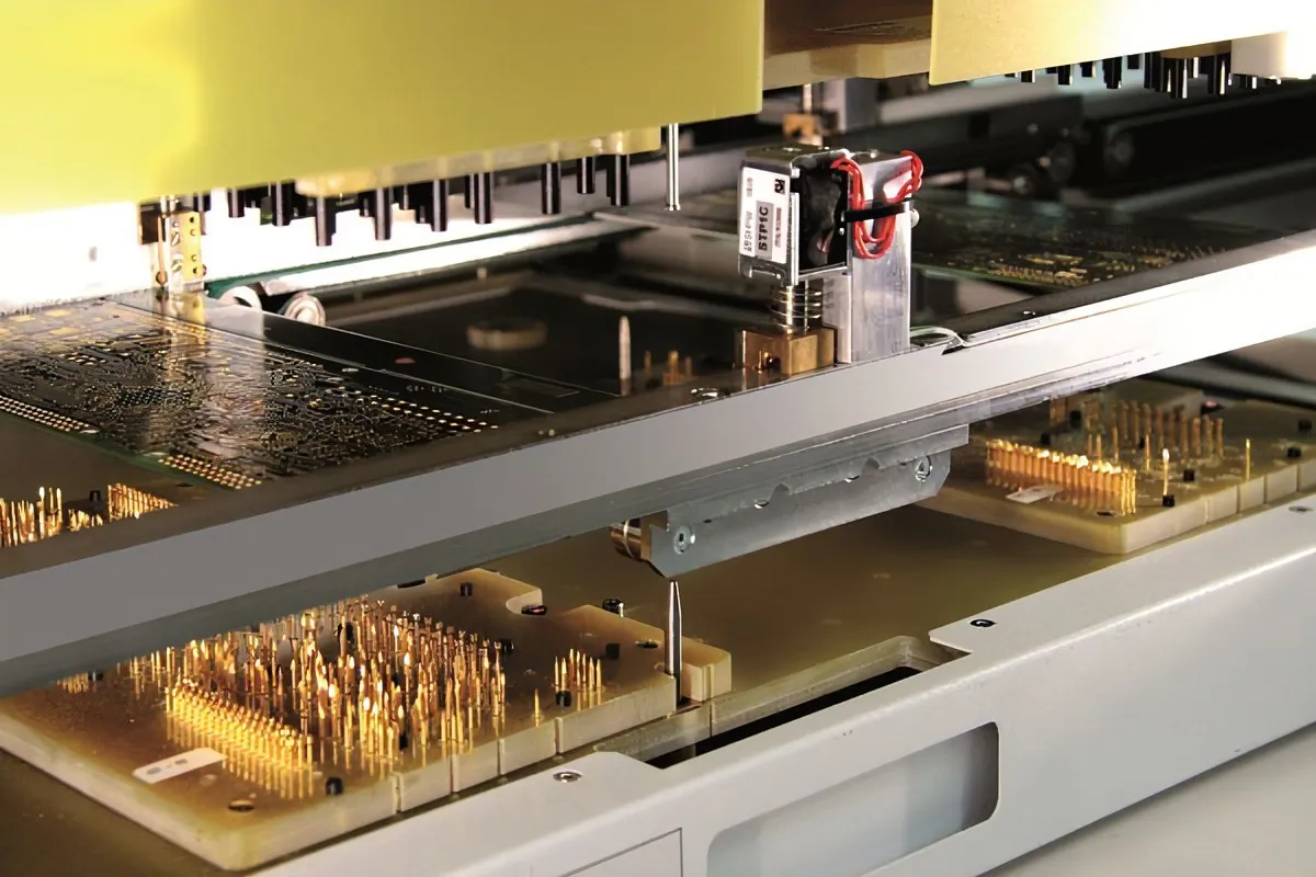
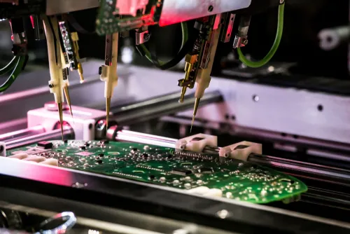
PCB testing methods vary by stage, from bare board fabrication to final assembly verification. Electrical testing dominates, including continuity checks to detect opens and shorts, alongside insulation resistance measurements to verify dielectric strength. Fixture-based in-circuit testing (ICT) uses bed-of-nails probes for high-volume production, offering speed but requiring custom fixtures that increase upfront costs. In contrast, flying probe systems employ movable probes for low-volume or prototype runs, providing flexibility without dedicated tooling, though at slower throughput rates.
A PCB testing methods comparison reveals trade-offs: ICT excels in parallel testing for dense boards, achieving higher fault coverage, while flying probes adapt to design changes seamlessly. Functional testing simulates operational conditions post-assembly, validating interactions among components, but demands comprehensive test vectors. Visual optical inspection (AOI) complements these by detecting solder defects or misalignments non-destructively. Engineers select methods based on volume, complexity, and budget, often combining them for layered assurance.
Essential PCB Measurement Equipment Guide
Selecting the right PCB measurement equipment ensures precise quantification of parameters like trace impedance, board thickness, and coplanarity. Multimeters and ohmmeters serve basic continuity and resistance checks, while LCR meters assess capacitance and inductance on nets. For high-frequency signals, time-domain reflectometers (TDR) measure impedance discontinuities critical in RF designs. Dimensional tools such as coordinate measuring machines (CMM) or laser profilometers quantify warpage and bow, adhering to tolerances specified in performance standards.
Hi-pot testers apply high voltage to confirm isolation between layers, preventing arcing in operation. Thermal chambers paired with data loggers evaluate coefficient of thermal expansion mismatches. A PCB measurement equipment guide emphasizes calibration and traceability to maintain accuracy. Integrating automated test equipment (ATE) streamlines workflows, minimizing human error in repetitive measurements.
Best Practices for PCB Testing
Best practices for PCB testing begin with design for testability (DFT), incorporating test points on every net and avoiding high-density areas without access. Standardize procedures across teams to enable repeatable results, documenting pass/fail criteria upfront. Perform bare board tests before assembly to catch fabrication issues early, transitioning to in-circuit and functional tests post-population. Maintain clean environments to prevent contamination-induced false positives during probing.
Environmental preconditioning, such as baking to remove moisture per JEDEC guidelines, precedes reliability tests. Calibrate equipment regularly and train operators on anomaly recognition. Implement statistical process control to track defect trends over lots. These steps not only boost yield but also align with PCB testing standards compliance, fostering supplier accountability.
Advanced PCB Measurement Techniques
Advanced PCB measurement techniques push beyond basics, employing X-ray inspection for hidden solder voids or barrel fills in vias. Acoustic microscopy detects delaminations or cracks non-destructively via ultrasound waves. Strain gauging monitors mechanical stress during reflow, guided by IPC/JEDEC protocols for process optimization. Thermal imaging reveals hot spots from poor thermal management, informing layout refinements.
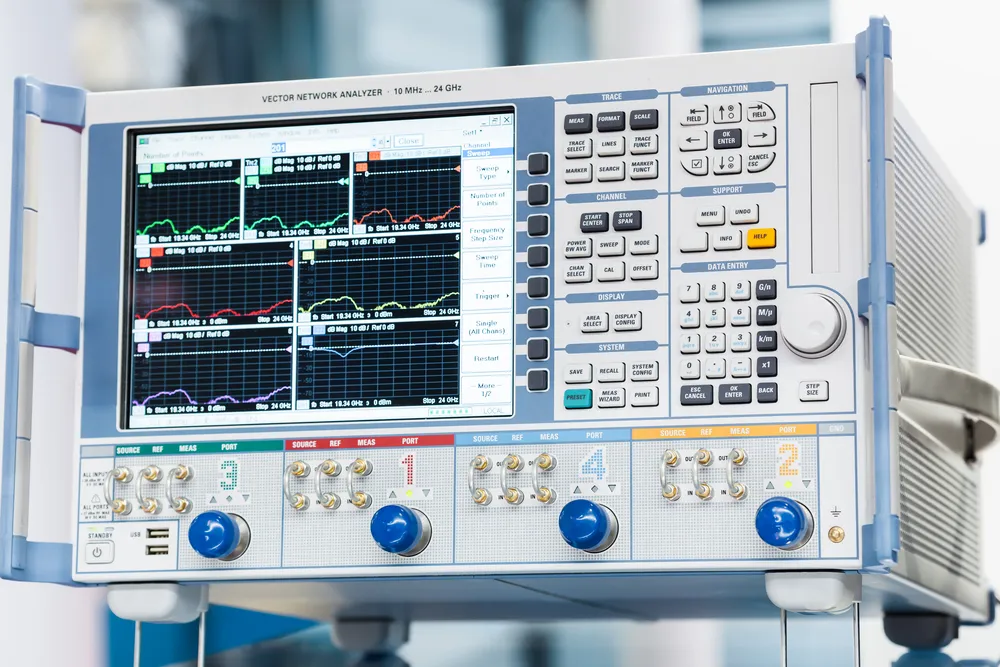
Boundary scan (JTAG) enables at-speed testing of digital logic without physical probes, ideal for complex BGA packages. For high-speed boards, vector network analyzers characterize S-parameters for signal integrity. These methods demand expertise but yield deeper insights into failure modes. Electrical engineers leverage them for next-generation designs, ensuring robustness in 5G and AI hardware.
Troubleshooting Common PCB Test Failures
When tests reveal issues, systematic root cause analysis is key. Continuity opens often trace to drill breakout or plating voids, resolvable by enhancing fabrication controls. Insulation failures signal contamination or under-etched clearances, mitigated through plasma cleaning. Warpage exceeding limits points to CTE mismatches between copper and substrate, addressed via symmetric stackups.
Solderability woes, assessed via wetting balance, stem from oxidation; steam aging restores surfaces. Functional discrepancies may arise from component tolerances or timing drifts, verified through oscilloscope captures. Documenting failure modes builds a knowledge base for iterative improvements. Collaborating with fabricators accelerates resolutions, upholding IPC-6012 performance specifications.
Conclusion
Test and measurement PCBs demand a multifaceted approach encompassing electrical validation, dimensional checks, and reliability assessments. Comparing methods like flying probe versus ICT guides efficient strategies tailored to production scales. Adhering to best practices for PCB testing, from DFT to calibration, ensures consistent quality. PCB testing standards compliance via IPC-TM-650 and JEDEC frameworks provides a universal benchmark. Advanced techniques like X-ray and strain analysis unlock superior performance. Electrical engineers equipped with this knowledge deliver reliable boards that power innovation.
FAQs
Q1: What is the best PCB testing methods comparison for high-volume production?
A1: Fixture-based in-circuit testing outperforms flying probe in speed and coverage for high-volume runs, using parallel probes on bed-of-nails setups. It detects opens, shorts, and passive values efficiently but requires custom fixtures. Flying probe suits prototypes with flexibility. Combine with AOI for comprehensive PCB testing methods comparison, ensuring standards compliance and yield optimization.
Q2: How does a PCB measurement equipment guide help in impedance control?
A2: A PCB measurement equipment guide recommends TDR or VNA for precise impedance profiling on high-speed traces. These tools identify mismatches from variations in width, height, or dielectric. Regular verification during fab maintains tolerances within 10% Z0. Integrate with design simulations for proactive adjustments, supporting advanced PCB measurement techniques.
Q3: What are best practices for PCB testing to achieve standards compliance?
A3: Best practices for PCB testing include DFT with ample test points, environmental preconditioning, and calibrated equipment per IPC guidelines. Sequence bare board electrical tests before assembly, logging data for traceability. Train teams on acceptability criteria to minimize escapes. This approach ensures PCB testing standards compliance, reducing field failures.
Q4: Which advanced PCB measurement techniques detect hidden defects?
A4: Advanced PCB measurement techniques like X-ray and acoustic microscopy reveal voids, cracks, or delaminations invisible to optical methods. Strain gauging quantifies reflow stresses, while thermal cycling simulates operation. These non-destructive tools enhance reliability analysis, ideal for multilayer boards in demanding applications.
References
IPC-TM-650 — Test Methods Manual. IPC, latest revision
IPC-6012E — Qualification and Performance Specification for Rigid Printed Boards. IPC, 2017
JEDEC J-STD-020E — Moisture/Reflow Sensitivity Classification of Nonhermetic Surface Mount Devices. JEDEC, 2014
IPC-A-600K — Acceptability of Printed Boards. IPC, 2020


