Introduction
Solar inverters represent a critical component in photovoltaic systems, efficiently converting variable DC output from solar panels into stable AC power for residential, commercial, or grid-scale applications. The PCB within a solar inverter must withstand high voltages up to 1000 V DC, currents exceeding 50 A, and switching frequencies in the tens of kHz range to achieve efficiencies above 98 percent. Poor PCB design can lead to overheating, electromagnetic interference, or premature failure, compromising system reliability and safety. High-performance PCB design considerations become essential to address these challenges, incorporating robust material choices, optimized layouts, and rigorous validation processes. For electric engineers, mastering solar inverter PCB design ensures compliance with industry expectations for longevity and performance in outdoor environments exposed to temperature swings from -40°C to 85°C and high humidity. This guide provides structured insights into best practices for PCB design, focusing on power electronics PCB design principles that drive superior outcomes.
Why High-Performance Solar Inverter PCBs Matter
Solar inverters operate continuously to maximize energy harvest, placing extraordinary demands on the PCB to handle power densities exceeding 10 W per square centimeter. A well-designed high-performance PCB minimizes losses from resistance and inductance, directly boosting overall inverter efficiency and reducing operational costs over a 25-year lifespan. Failures in PCB design considerations, such as inadequate thermal paths or excessive EMI, can trigger shutdowns, void warranties, and increase maintenance expenses. In power electronics PCB design, the PCB must support advanced topologies like three-phase bridges with SiC or GaN switches, requiring precise control of parasitics for minimal ringing and voltage overshoot. Engineers prioritize these aspects to meet grid synchronization standards and ensure seamless integration with maximum power point tracking algorithms. Ultimately, superior solar inverter PCB design translates to higher return on investment for renewable energy deployments.
Fundamental Technical Principles in Solar Inverter PCB Design
The core of solar inverter PCB design revolves around managing power flow through topologies such as H-bridges or resonant converters, where fast switching generates significant heat and electromagnetic fields. High-frequency operation necessitates low-inductance paths to prevent voltage spikes that could damage semiconductors, achieved by shortening current loops and paralleling traces. Material selection influences dielectric strength and thermal conductivity, with FR-4 variants often augmented by higher-performance resins for elevated operating temperatures. Layer stackup plays a pivotal role, separating high-current power layers from sensitive control signals to preserve integrity. Creepage and clearance distances must account for pollution degrees and overvoltages, preventing arcing in humid coastal installations. These principles form the foundation for reliable high-performance PCBs in demanding solar applications.
Key PCB Design Considerations for Solar Inverters
Material Selection and Stackup Optimization
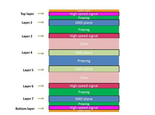
Selecting laminates with high glass transition temperature (Tg above 170°C) ensures stability during thermal cycling from power surges. Thick copper foils, from 2 oz to 6 oz per square foot, accommodate high currents while minimizing I2R losses in power traces. Multilayer configurations, typically 8 to 16 layers, dedicate inner planes for power distribution and return paths, enhancing current carrying capacity. Vias must be plated generously to handle thermal expansion without cracking. Adherence to IPC-2221 guidelines for laminate qualification prevents delamination under prolonged exposure. This structured approach to stackup optimizes both electrical and mechanical performance.
Thermal Management Strategies
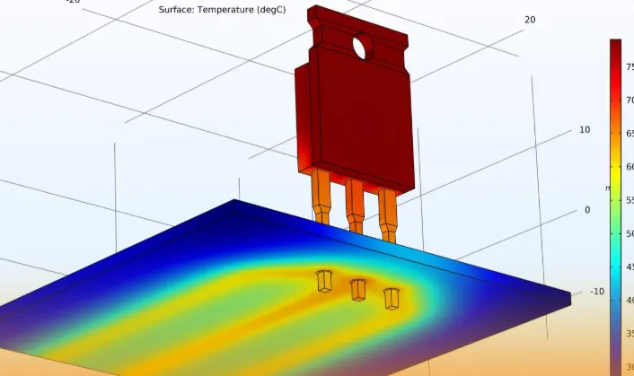
Effective heat dissipation is paramount, as power devices like IGBTs or MOSFETs generate junction temperatures that must stay below 150°C. Thermal vias arrays under hotspots transfer heat to opposite layers or embedded heat spreaders, increasing effective conductivity by factors of 5 to 10 times. Component placement clusters high-loss elements centrally for uniform airflow from forced convection cooling. Copper pours and filled vias act as heat pipes, distributing flux evenly across the board. Simulations verify junction-to-ambient resistance below 1°C/W, guiding heatsink sizing. These practices sustain peak performance without derating.
High-Current Trace and Via Design
Power traces require widths calculated for temperature rises under full load, often exceeding 10 mm for 100 A paths. Paralleling multiple traces or using bus bars reduces resistance and inductance. Via fields, with 0.3 mm drills and 1 oz plating, bridge layers without bottlenecks. Solder mask cutouts expose copper for direct cooling. IPC-2152 charts provide conservative sizing to avoid hotspots exceeding 20°C rise. Precision in these elements prevents electromigration over millions of cycles.
EMI Mitigation and Signal Integrity
Switching edges with di/dt over 100 A/μs radiate noise, necessitating solid ground planes to contain fields. Critical loops for gate drive and DC link capacitors shrink to millimeters, with twisted pairs for control signals. Guard traces and stitching vias shield analog sections from digital noise. Ferrite beads suppress common-mode currents on inputs. Layer sequencing places power ground adjacent to signal ground, connected at single points. These techniques ensure compliance with emission limits.
High-Voltage Isolation and Safety
Creepage distances scale with working voltage and contamination levels, often 8 mm per 1000 V RMS. Slots or grooves in solder mask enhance insulation resistance above 100 MΩ. Optocouplers and transformers isolate control from power sections. Partial discharge testing validates designs under 80 percent overvoltage. Conformal coatings add 200 percent creepage effectively. IEC 62109 requirements for photovoltaic converters underscore these isolation imperatives.
Best Practices for PCB Design in Solar Inverters
Implement design rules checking early to enforce minimum clearances and trace widths. Prototype with impedance-controlled fabrication to validate parasitics before production. Finite element analysis for thermal hotspots refines layouts iteratively. Controlled impedance for gate drives maintains switching speeds. Factory acceptance tests simulate field conditions like 85°C/85% RH aging. Documentation includes gerber files with fab notes specifying heavy copper etching and sequential lamination. Collaboration with fabricators ensures DFM compliance from inception.
Power plane splits avoid resonance at switching harmonics. Decoupling capacitors place within 5 mm of IC pins. Solder joints for power devices use vapor phase reflow for void-free connections. Reliability predictions via accelerated life testing project MTBF beyond 100,000 hours. These best practices for PCB design elevate solar inverter PCB design to production-ready levels.
Common Challenges and Troubleshooting Insights
Overheating often stems from undersized vias; remedy by increasing density and plating thickness. EMI failures trace to long gate loops; shorten with dedicated drive layers. Warpage in thick boards arises from asymmetric copper; balance with blind vias. Solderability issues on heavy copper demand HASL alternatives like ENIG. Vibration-induced cracks in BGA packages require underfill. Post-mortem analysis via X-ray and cross-sectioning informs revisions. Logical root cause methods accelerate resolutions.
(Insert image: 'PCB Warpage Measurement' · ALT: 'Dial gauge setup testing warpage on a high-performance power electronics PCB')
Conclusion
Designing a high-performance solar inverter PCB demands integrated attention to thermal, electrical, and mechanical factors for unwavering reliability. By prioritizing robust stackups, precise trace sizing, and EMI controls, engineers achieve efficiencies and lifespans that underpin sustainable energy goals. Adopting these PCB design considerations and best practices for PCB design positions projects for success amid rising solar adoption. Future advancements in materials will further refine power electronics PCB design, but foundational principles remain timeless. Electric engineers equipped with this knowledge deliver systems that perform exceptionally in real-world deployments.
FAQs
Q1: What are the primary PCB design considerations for solar inverters?
A1: Solar inverter PCB design must address high-current handling, thermal dissipation, and voltage isolation to manage power conversion efficiently. Key factors include wide traces per IPC-2221, thermal vias arrays, and multilayer stackups separating power from signals. These ensure low losses and reliability under variable loads. Optimizing component placement near cooling enhances performance further.
Q2: How does thermal management impact high-performance PCB design?
A2: Thermal management prevents device degradation in solar inverters by maintaining temperatures below critical thresholds. Practices like copper pours, embedded heat spreaders, and airflow-optimized layouts reduce junction temperatures effectively. Simulations guide via placement for even heat spreading. This sustains efficiency over extended operations in hot climates.
Q3: What best practices minimize EMI in power electronics PCB design?
A3: Best practices for PCB design include minimizing high di/dt loop areas, using contiguous ground planes, and shielding sensitive traces. Stitching vias and guard rings contain emissions from switching elements. Layer adjacency for power and ground returns improves return paths. These steps ensure quiet operation alongside grid compliance.
Q4: Why is layer stackup critical in solar inverter PCB design?
A4: Layer stackup in high-performance PCBs facilitates power plane integrity and signal isolation, reducing inductance in DC links. Dedicated planes handle ripple currents without voltage droop. Symmetric builds prevent warpage during reflow. This configuration supports high-frequency switching with minimal parasitics for optimal efficiency.
References
[1] https://www.pcbonline.com/blog/Solar-Inverter-Circuit-Boards-Design.html
[2] https://www.protoexpress.com/blog/pcb-layout-design-tips-for-power-electronics
[3] https://www.allpcb.com/blog/pcb-knowledge/designing-high-efficiency-solar-pcbs-balancing-power-and-thermal-management.html
[4] https://www.allpcb.com/blog/pcb-knowledge/thermal-management-in-pcbs.html
[5] https://www.pcbway.com/blog/PCB_Design_Layout/Inverter_PCB_Layout_Guidelines_Best_Practices_for_High_Efficiency_and_Low_EMI_P_b42d1a52.html
[6] https://www.pcbpower.us/blog/pcb-for-power-electronics-a-design-guide
[7] https://www.viasion.com/blog/a-guide-to-inverter-pcb-design-and-layout
IPC-2221B — Generic Standard on Printed Board Design. IPC, 2012
IPC-6012E — Qualification and Performance Specification for Rigid Printed Boards. IPC, 2017
IEC 62109-1 — Safety of power converters for use in photovoltaic power systems. Part 1: General requirements. IEC, 2010


