Introduction
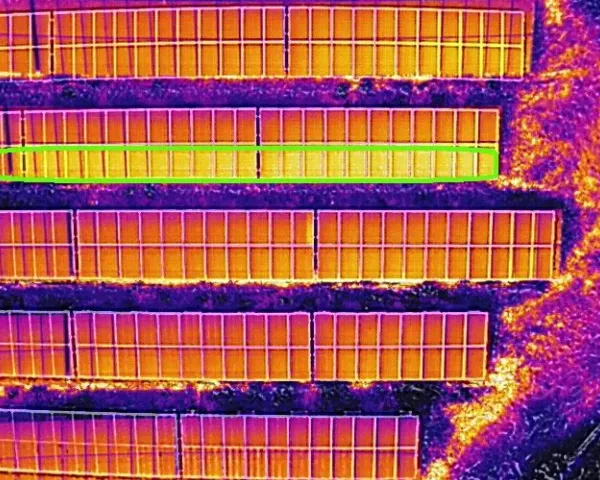
Solar inverters convert direct current from photovoltaic panels into alternating current for grid or home use, operating under demanding conditions with high power levels and variable environmental stresses. In these systems, printed circuit boards (PCBs) host critical power electronics that generate substantial heat during conversion processes. Effective solar inverter PCB thermal management becomes essential to prevent overheating, which can degrade components, reduce efficiency, and shorten operational life. Poor heat dissipation leads to thermal runaway, electromigration in traces, and delamination of laminates, compromising system reliability in outdoor installations exposed to elevated ambient temperatures and solar loading.
Engineers designing these PCBs must prioritize thermal pathways from heat-generating elements like switching transistors and diodes to ambient air or external cooling structures. PCB heat dissipation strategies directly influence inverter efficiency, often targeting minimal power losses while adhering to performance specifications. This article explores the principles, challenges, and solutions for thermal management in solar inverter PCBs, emphasizing structured approaches that ensure longevity and reliability for electric engineers.
Why Thermal Management Matters in Solar Inverter PCBs
Solar inverters handle peak power demands during midday sunlight, subjecting PCBs to continuous thermal cycling from diurnal temperature swings and load variations. Heat accumulation stresses solder joints, capacitors, and semiconductors, accelerating failure mechanisms such as creep and fatigue. Solar inverter PCB thermal management directly impacts overall system uptime, as inverters represent a common point of failure in photovoltaic arrays due to thermal-related degradation.
Reliability data from field deployments highlight that inadequate PCB heat dissipation correlates with reduced inverter lifespans, often below 20 years in harsh climates. Engineers must balance compact layouts for cost-effective enclosures with sufficient thermal margins to maintain junction temperatures within safe operating limits. Standards like IPC-2221 provide guidelines for designing PCBs that accommodate power densities typical in inverters, ensuring mechanical integrity under thermal loads.
Moreover, efficient thermal design enhances energy conversion efficiency by minimizing resistive losses exacerbated by elevated temperatures. Procurement teams specify thermal performance in PCB requirements to align with inverter warranties, while designers simulate worst-case scenarios to validate choices early.
Heat Generation and Transfer Mechanisms in Solar Inverter PCBs
Power semiconductors in solar inverters, such as insulated gate bipolar transistors and metal-oxide-semiconductor field-effect transistors, dissipate heat primarily through conduction losses during switching and on-state resistance. Diodes and inductors contribute additional joule heating, concentrating thermal energy at specific board locations. Radiation and convection play secondary roles, but conduction via copper traces and planes dominates initial heat spreading within the PCB stackup.
Heat transfer occurs through three modes: conduction along metal paths and dielectric layers, convection to surrounding air or forced airflow, and radiation from hot surfaces. In multilayer boards, inner layers act as thermal reservoirs, but low-conductivity laminates limit spreading unless augmented by vias. Engineers model these mechanisms to predict hotspots, where localized temperatures exceed component ratings, leading to accelerated aging.
Thermal impedance, quantified as the temperature rise per watt, guides design trade-offs between trace width, layer count, and material properties. JEDEC standards like JESD51 series define test boards for characterizing package-to-ambient thermal resistance, aiding comparisons across configurations. Understanding these principles allows precise allocation of thermal budgets across the inverter circuitry.
Key Challenges in PCB Heat Dissipation for Solar Inverters
High power densities in modern inverters exceed 20 kW per unit, amplifying heat flux on PCBs and challenging passive dissipation alone. Enclosure constraints limit airflow, forcing reliance on conduction to chassis-mounted heatsinks. Variable ambient conditions, from freezing nights to scorching days, induce expansion mismatches between copper and substrates, risking cracks under IPC-6012 performance criteria.
Component packaging evolves toward bottom-terminated devices, complicating direct heatsink attachment and increasing reliance on board-level spreading. Electromagnetic compatibility requirements often dictate ground plane segmentation, fragmenting thermal paths. Engineers face trade-offs where wider traces for current capacity per IPC-2221 also serve heat spreading, but multilayer complexity demands simulation to verify efficacy.
Dust accumulation in field installations further impairs convection, underscoring the need for robust conduction-focused designs. These challenges necessitate integrated approaches combining layout, materials, and simulation.
Practical Solutions for Effective Thermal Management
Selecting High-Temperature PCB Materials
High-temperature PCB materials resist degradation from prolonged exposure, maintaining dielectric integrity and mechanical strength. Laminates with elevated glass transition temperatures prevent softening during reflow or operation, while low coefficients of thermal expansion minimize warpage. For solar inverters, these materials support stackups handling power stages without via barrel cracking.
Ceramic-filled or metal-core constructions enhance through-plane conductivity, ideal for direct heatsink bonding. Copper-invar-copper cores balance expansion for hybrid assemblies. Material selection aligns with application demands, prioritizing thermal conductivity over cost for critical sections.
Optimizing PCB Heat Dissipation Through Layout
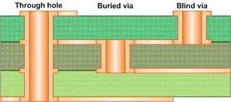
Strategic component placement positions heat sources centrally for even spreading, avoiding board edges where convection weakens. Wide polygons on outer layers act as spreaders, channeling heat to multiple vias arrays. Filled or staggered vias under packages transfer heat vertically, with pitch and diameter optimized for flow without drill smear.
Copper balance across layers equalizes temperatures, reducing gradients that stress vias. Ground planes, when continuous, double as heat sinks, but splits for noise require compensatory thickening. Airflow paths remain unobstructed, directing cooling over hotspots.
Heat Sink Design for PCBs
Heat sink design for PCBs integrates fins or pins directly bonded via thermal interface materials to exposed copper pads. Pin-fin arrays suit forced convection in inverter fans, maximizing surface area per footprint. Extruded aluminum profiles attach via screws or clips, ensuring low thermal resistance junctions. Incorporating a solar inverter PCB thermal management guide into the design workflow helps engineers systematically address high-power losses, junction heating, and long-term reliability in energy conversion systems.
Embedded heat pipes or vapor chambers handle extreme densities, capillary action distributing heat laterally. Interface gaps below 50 microns prevent hotspots, verified post-assembly. Design iterates with finite element models to match sink profiles to PCB hotspots.
Leveraging Thermal Simulation for PCBs
Thermal simulation for PCBs predicts steady-state and transient profiles, iterating designs pre-prototype. Finite difference or element methods solve conduction equations across geometries, incorporating material libraries and boundary conditions like convection coefficients. Junction temperatures guide derating, ensuring margins under maximum solar irradiance.
Coupled electro-thermal analysis captures switching losses dynamically. Validation against JEDEC test boards calibrates models, bridging simulation to physical tests. This front-loading reduces revisions, accelerating time-to-market.
Troubleshooting Common Thermal Issues
Overheating often traces to undersized traces per power levels, inflating resistance and self-heating. Inspect via infrared thermography post-assembly to map discrepancies against simulations. Delamination signals moisture ingress or Tg exceedance, prompting bake-out and material upgrades.
Vias plugging from plating reduces conductivity; microsectioning confirms fill quality. Fan failure amplifies reliance on conduction, necessitating redundant paths. Field returns correlate with underspecified interfaces, emphasizing compression testing.
Conclusion
Solar inverter PCB thermal management underpins reliable power conversion amid rising photovoltaic adoption. From material choices and layout optimizations to heat sink design for PCBs and thermal simulation for PCBs, integrated strategies mitigate risks effectively. Adhering to standards like IPC-2221 and JEDEC JESD51 ensures designs withstand real-world stresses, extending inverter lifespans.
Engineers gain longevity through proactive dissipation, balancing performance with manufacturability. Future advancements in nanomaterials promise further gains, but fundamentals remain paramount.
FAQs
Q1: What are the primary methods for PCB heat dissipation in solar inverters?
A1: PCB heat dissipation relies on copper planes for spreading, thermal vias for interlayer transfer, and convection to heatsinks. Layouts position sources for optimal airflow, while high copper weights enhance conduction. These align with design guidelines to manage power losses efficiently.
Q2: How does heat sink design for PCBs improve solar inverter reliability?
A2: Heat sink design for PCBs uses fins to increase surface area, bonded via low-resistance interfaces. This lowers junction temperatures, preventing thermal runaway in power devices. Proper profiling matches PCB hotspots, validated through testing for sustained performance.
Q3: Why use thermal simulation for PCBs in solar inverter design?
A3: Thermal simulation for PCBs forecasts hotspots under load, enabling layout refinements early. It incorporates convection and conduction, derating components accurately. This reduces prototypes and ensures compliance with thermal specifications.
Q4: What role do high-temperature PCB materials play in inverters?
A4: High-temperature PCB materials resist softening and warpage, supporting dense power layouts. They maintain integrity during cycling, minimizing electromigration risks. Selection focuses on thermal conductivity for effective dissipation in harsh environments.
References
IPC-2221B - Generic Standard on Printed Board Design. IPC, 2012
IPC-6012DS - Qualification and Performance Specification for Rigid Printed Boards. IPC, 2015
JEDEC JESD51-7 - High Effective Thermal Conductivity Test Board for Leaded Surface Mount Packages. JEDEC, 2004
IEC 62109-1 - Safety of power converters for use in photovoltaic power systems - Part 1: General requirements. IEC, 2010


