Introduction
Insulin pumps represent a cornerstone of modern diabetes management, delivering precise doses of insulin continuously to maintain stable blood glucose levels. At the heart of these devices lies the printed circuit board (PCB), which orchestrates sensors, microcontrollers, pumps, and communication interfaces in a compact, wearable form factor. For electrical engineers tasked with insulin pump PCB design rules, the stakes are exceptionally high, as any failure could lead to life-threatening consequences. This article explores the medical PCB design constraints that ensure reliability, safety, and performance in these life-critical applications. By adhering to high-reliability PCB design principles, engineers can mitigate risks associated with electrical, mechanical, and environmental stresses. Understanding these considerations enables the creation of robust systems compliant with stringent regulatory frameworks.
The Critical Role of PCBs in Insulin Pumps
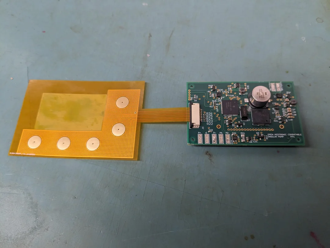
Insulin pumps must operate flawlessly for extended periods, often 24/7, while exposed to body temperature, moisture, and mechanical movement from daily activities. The PCB serves as the central nervous system, integrating low-power analog circuits for glucose sensing, digital control for dosing algorithms, and power management for battery efficiency. In PCB design for life-critical applications, even minor defects like delamination or trace fractures can cascade into dosing errors or device failure. Engineers must prioritize materials and layouts that withstand thermal cycling, vibration, and humidity without compromising signal integrity. This demands a shift from standard consumer electronics practices to those emphasizing redundancy and fault tolerance. Ultimately, the PCB's design directly influences the device's mean time between failures, a key metric in high-reliability PCB design.
Key Medical PCB Design Constraints
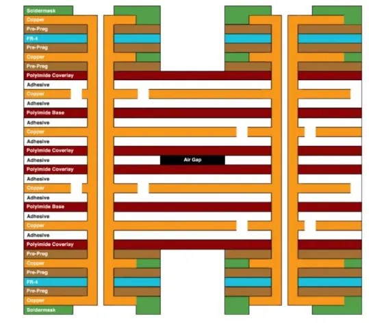
Medical PCB design constraints begin with spatial limitations, as insulin pumps prioritize portability and patient comfort, often requiring boards smaller than 50 square centimeters. Multilayer stackups with fine-pitch traces and microvias enable dense integration but introduce challenges like crosstalk and impedance control. Environmental factors, including constant proximity to skin and sweat, necessitate materials with low moisture absorption and high glass transition temperatures to prevent warpage. Power constraints from coin-cell or lithium-polymer batteries demand efficient DC-DC converters and sleep modes to extend operational life. Mechanical stresses from pump actuation require reinforced vias and anchor points to avoid microcracks. These constraints shape every aspect of insulin pump PCB design rules, from component placement to solder joint integrity.
High-Reliability PCB Design Principles
High-reliability PCB design starts with material selection, favoring laminates with controlled coefficient of thermal expansion to match component leads and minimize solder joint stress during assembly and operation. Controlled impedance traces ensure signal fidelity for precise analog-to-digital conversions in glucose monitoring circuits. Via reliability becomes paramount, with filled or staggered vias preferred to handle current densities without electromigration. Ground planes and stitching vias suppress electromagnetic interference, critical for wireless communication modules in pumps. Redundant routing paths provide failover options in case of trace failures. These principles align with IPC Class 3 requirements, ensuring the board meets performance specs under harsh conditions typical of life-critical applications.
IEC 60601 PCB Compliance Essentials
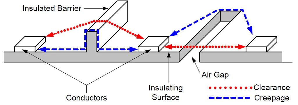
IEC 60601 compliance mandates specific insulation distances on PCBs to prevent electrical hazards in patient-contact devices. Creepage and clearance distances must account for working voltage, pollution degree, and material group, often requiring wider spacing or slots between high-voltage traces and patient-accessible parts. Dielectric strength testing verifies barrier integrity against breakdown. Leakage current paths demand careful grounding schemes, separating protective earth from signal grounds. Component spacing rules extend to optocouplers and transformers for galvanic isolation. Engineers verify these through design rule checks and simulation before prototyping, integrating IEC 60601 PCB compliance into the earliest stages of insulin pump PCB design rules.
Thermal and Power Management in Compact Designs
Thermal management poses unique challenges in insulin pumps, where body heat and low airflow limit dissipation. Power planes and thermal vias distribute heat from processors and drivers evenly, preventing hotspots that could degrade components over time. Low-power design rules minimize quiescent currents, with careful decoupling capacitor placement to stabilize supplies. Battery monitoring circuits require robust protection against over-discharge and short circuits. Finite element analysis helps predict junction temperatures during basal and bolus modes. These strategies ensure sustained performance without compromising the compact form factor essential for wearability.
EMI/EMC and Signal Integrity Considerations
Electromagnetic compatibility is non-negotiable, as pumps integrate RF for data upload and must avoid interfering with or from other medical devices. Shielded enclosures and filtered connectors contain emissions, while PCB-level shielding via ground pours reduces radiated noise. Differential pair routing with length matching preserves timing for high-speed interfaces. Crosstalk mitigation involves guard traces and orthogonal routing layers. Pre-compliance testing identifies issues early. In high-reliability PCB design, these measures safeguard against false readings or communication dropouts that could disrupt therapy.
Practical Best Practices for Implementation
Adopt design for manufacturability by specifying IPC Class 3 tolerances for trace width, annular ring, and hole wall quality. Use high-temperature solders resistant to lead-free reflow profiles, ensuring joint reliability under vibration. Implement automated optical inspection and X-ray for hidden defects post-assembly. Qualification testing includes thermal cycling, humidity bias, and mechanical shock per relevant standards. Documentation traces compliance throughout the lifecycle. These best practices streamline medical PCB design constraints into production-ready insulin pump PCB design rules.
Troubleshooting Common Issues
Warpage from mismatched CTE often manifests as assembly defects; mitigate with symmetric stackups and low-CTE cores. Solder voids under BGAs signal reflow profile issues, addressed by vapor phase soldering for uniform heating. Signal noise in analog sections traces to poor grounding; star-point schemes resolve this. Firmware glitches mimicking hardware faults require design-in debug headers. Iterative DFMEA identifies root causes systematically. Troubleshooting reinforces PCB design for life-critical applications.
Conclusion
Designing PCBs for insulin pumps demands a holistic approach balancing compactness, reliability, and safety under IEC 60601 PCB compliance and high-reliability PCB design tenets. Electrical engineers must integrate material science, layout precision, and rigorous verification to deliver devices that perform flawlessly in real-world use. Key takeaways include prioritizing creepage distances, thermal control, and EMI shielding while adhering to IPC Class 3 standards. These considerations not only meet medical PCB design constraints but elevate patient outcomes. Future advancements in HDI and flexible substrates will further refine insulin pump PCB design rules, pushing the boundaries of wearable medical technology.
FAQs
Q1: What are the primary insulin pump PCB design rules for high reliability?
A1: Insulin pump PCB design rules emphasize IPC Class 3 fabrication tolerances, symmetric stackups to control warpage, and redundant power routing. Creepage distances per IEC 60601 prevent leakage currents, while thermal vias manage heat from integrated circuits. Low-moisture materials ensure stability in humid environments. These rules support continuous operation essential for basal insulin delivery. Verification through accelerated life testing confirms long-term performance.
Q2: How do medical PCB design constraints impact layout in life-critical applications?
A2: Medical PCB design constraints dictate wider trace spacing for insulation, compact HDI for miniaturization, and isolated power domains to limit fault propagation. Vibration-resistant vias and flexible interconnects accommodate pump mechanics. EMI shielding layers protect sensitive sensors. Compliance with standards like IEC 60601 integrates safety into every decision. Engineers balance density with robustness for wearable form factors.
Q3: Why is IEC 60601 PCB compliance crucial for insulin pumps?
A3: IEC 60601 PCB compliance ensures electrical safety through defined creepage, clearance, and dielectric requirements, mitigating shock risks in patient-applied parts. It mandates testing for essential performance under fault conditions. Grounding hierarchies prevent hazardous potentials. For insulin pumps, this safeguards precise dosing against electrical anomalies. Non-compliance risks regulatory rejection and patient harm.
Q4: What role does high-reliability PCB design play in PCB design for life-critical applications?
A4: High-reliability PCB design employs premium laminates, fine-pitch capabilities, and rigorous qualification to achieve MTBF exceeding device lifespan. It addresses electromigration, delamination, and ionic contamination proactively. Redundancy and monitoring circuits enhance fault tolerance. In insulin pumps, this translates to uninterrupted therapy delivery. Standards like IPC-6012 guide qualification for mission-critical use.
References
IEC 60601-1 — Medical electrical equipment - Part 1: General requirements for basic safety and essential performance. IEC, 2005
IPC-6012E — Qualification and Performance Specification for Rigid Printed Boards. IPC, 2015
IPC-A-610F — Acceptability of Electronic Assemblies. IPC, 2014


